Research Article
Effect of Vanadium on Structure and Morphology of SnO2 Thin Films
Shawki Khalaph Muhammad 1, Ehssan Salah Hassan 2, Kameran Yasseen Qader 3, Khalid Haneen Abass 4, Sami Salman Chiad 3, Nadir Fadhil Habubi 3*
1 Department of Physics, College of Girl Education, Kufa University, Iraq.
2 Department of Physics, College of Science, Mustansiriyah University, Baghdad, Iraq.
3 Department of Physics, College of Education, Mustansiriyah University, Baghdad, Iraq.
4 Department of Physics, College of Education for Pure Sciences, University of Babylon, Iraq.
* Corresponding author. E-mail: nadirfadhil@uomustansiriyah.edu.iq
Received: Sep. 26, 2019; Accepted: Feb. 22, 2020; Published: Feb. 24, 2020
Citation: Shawki Khalaph Muhammad, Ehssan Salah Hassan, Kameran Yasseen Qader, Khalid Haneen Abass, Sami Salman Chiad, and Nadir Fadhil Habubi, Effect of Vanadium on Structure and Morphology of SnO2 Thin Films. Nano Biomed. Eng., 2020, 12(1): 67-74.
DOI: 10.5101/nbe.v12i1.p67-74.
Abstract
Tin oxide was prepared by chemical methods and then doped with different weight ratios of vanadium 2wt% and 4wt%. The structural, morphological, and optical properties were studied. It was found that all the recorded films had a polycrystalline diffraction pattern and that the predominant reflection was (111) plane. The doping processes resulted in the improvement of crystalline structure and the disappearance of a number of secondary reflections and the direction of the film in a single crystalline pattern, thus reducing the values of energy gap and percentage transmittance. The morphological properties were studied by converting the three-dimensional images into graphic drawings to enable us to easily calculate surface parameters.
Keywords: Vanadium; Chemical spray; Grain bindery; Conical; Tin oxide
Introduction
The process of doping metal oxides semiconductors with the transition metals of the second group in the periodic table or their ions is considered as an important and interesting subject in many fields of applications [1], such as gas sensors [2], surface coatings, environmental and human health [3], organic pollutants and toxic water [4], photocatalysis [5], probe reaction to evaluate the catalytic activity [6], and nanocomposite or heterojunction catalysts [7]. Where a small amount of material from the transition group can have a significant and a clear effect on the properties of surface electrical conductivity [8]. Tin dioxide was doped successfully with different transition metals such as cobalt [9], nickel [10], chromium [11], iron [12] and magnesium [13]. Where tin oxide has a wide band gap of 3.6 eV at a temperature of 300k [14], SnO2 is a semiconductor of n type [15]. The precipitated tin oxide with vanadium was studied, which increased the sensitivity of CO gas because of the development of V+3, V+4, V+5 [16]. The effect of addition of vanadium to SnO2 was also studied, and it was found that V+4 ions were the best performance of V+5 for H2, which reduced the oxygen vacancies on the surface and reduced the degree of crystallization [17]. Vanadium was added to SnO2 for the purpose of measuring the sensitivity of the prepared film to SO2 sulfur dioxide at a concentration of 5 ppm. Sensitivity percentage was 70% when adding 15wt% to SnO2 at the concentration of gas 100 ppm of SO2. For 5 ppm of SO2 gas, sensitivity percentage was 45% in the same doping weight ratio [18]. The aim of this work was to prepare vanadium doped SnO2 in order to study its structural, morphological and optical properties.
Experimental
The experimental setup was discussed elesewhere [19]. 0.1 M of SnCl4. 5H2O was dissolved in deionized water to prepare undoped SnO2 provided by Sigma-Aldrich – German. The doping agent was vanadium (III) chloride VCl3 in deionized water to prepare V doped SnO2 provided by Sigma-Aldrich – German. A few drops of HCl were added to the solution in order to get a clear solution. Substrate was glass slide. The preparation conditions: Substrate temperature was 450 ℃; distance between nozzle and substrate was 29 cm; spraying period 10 s lasted by 90 s to avoid cooling; spray rate was 5 mL/min; nitrogen gas was used as a carrier gas. X-ray diffraction (XRD) (SHIMADZU XRD-6000), scanning electron microscope (SEM) (Jeol JSM 6335F), and transmission electron microscopy (TEM) (Type CM10 PW6020, Philips-Germany) were applied. Atomic force microscopy (AFM) was used to introduce surface topography using a digital tool Nanoscope Ш and Dimension 3100. Ultraviolet-visible spectrophotometer (UV Spectrophotometer Shimadzu Model UV-1800) was used to record the absorbance spectra in the wavelength range 200-1000 nm.
Results and Discussion
Fig. 1 represents an X-ray diffraction pattern of SnO2 precipitated by chemical spray technique and doped with vanadium by 2 and 4wt% on the glass substrate. It was noted from the figure that all the undoped and doped films were of a polycrystalline pattern. The dominant reflection was the (111) plane at angle 2θ = 30.02°that satisfied orthorhombic SnO2 (JCPDS 29- 1484) [20]. The intensity of this reflection increased with the increase of doping and decreased the full width at half maximum (FWHM) as shown in Fig. 1(a) [21] due to improvement in the crystallization. Increase in the intensity of the dominant (111) reflection was due to the fact that the ions radius of the dopant V+4 = 0.58 Å occupied interstitial sites due to the small ionic radius of the dopant ion compared to the host material Sn+4 = 0.71 Å, and therefore moving towards superlattice, which increased the transmittance due to the increase in grain size, leading to reducing grain boundaries that acted as centers of radiation dispersion. The inset-attached shapes represented the distribution of grain size, with grain boundaries by different colors for the purpose of clarifying the increase of these grains, indicating the improvement of the crystallization with increasing the intensity of reflection and increasing the crystalline size calculated by Sherrer’s formula Eq. 1 [22, 23]. Where the crystallite size increased from 19.35 to 37.78 nm when increasing the doping from 0wt% to 4wt% of vanadium, the number of secondary reflections at (020), (021), (022), (023), (041) corresponded to the angles 31.43°, 35.76°, 47.35°, 62.54° and 67.63°. All the diffraction peaks could be related to the tetragonal rutile structure of SnO2 and no reflections from vanadium oxide phases could be noticed. It was observed that the reflection (041) was only present in the undoped SnO2 and the reflection (022) and (023) disappeared at the 4wt% of vanadium. The reflection (021) and (021) decreased their intensity with doping and the doping matter improved crystallization significantly, with the film direction to a single crystalline pattern. Fig. 2(a), (b), (c) and (d) represents the full width at half maximum, crystallite size, microstrain and the dislocation density as a function of doping weight ratios. The opposite relationship between the FWHM and crystallite size was observed from Fig. 2(a) and (b) based on the Sherrer Equation (1). Fig. 2(c) represents the microstrain that was calculated by Equation (2), which was observed to decrease with doping due to improved crystallization of the deposited film. Fig. 2 (c) represents the dislocation density that was calculated by Equation (2), which also showed the decrease in their values due to the regular arrangement of crystalline and reduced the crystalline defects in the films. The unit cell (a, b and c) of the polycrystalline SnO2 films with (111) orientation was calculated using Equation (4) [24] and found good agreement with those reported in JCPDS standard data as shown in Table 1.
![]() (1)
(1)
![]() (2)
(2)
![]() (3)
(3)
![]() (4)
(4)
Fig. 3(a) represents a two-dimensional scanning electron microscope (SEM) image. Fig. 3(b) is a picture of a specific and amplified area of the film surface of Fig. 3(a) and different colors showing particle size using a professional program to calculate the surface parameters. Fig. 3(c) shows a graph of the distribution of surface heights of a specific area. All these figures described undoped thin films. It was noticed that surface of the films was homogeneous with some cracks and that the size of particles was close to each other, as was observed from the size of the colors as about 70 nm. The height histogram indicated that the height was distributed causally at the dominant height 125 nm.
Fig. 4(a) represents a two-dimensional SEM image. Fig. 4(b) is a picture of a specific and amplified area of the film surface of Fig. 4(a) with different colors showing particle size of Fig. 4(c), a graph of the distribution of surface heights of a specific area. All these figures described 2wt% vanadium doped SnO2 thin films. It was noticed that the surface of the films was homogeneous and the cracks became very few due to increased deflection, and that the size of the particles was close to each other They became larger due to increased crystallization, as was observed from the size of the colors as about 80 nm. The height histogram indicated that the height was Gaussian distributed at the dominant height 140 nm. Fig. 5(a) represents a two-dimensional SEM image. Fig. 5(b) is a picture of a specific and amplified area of the film surface of Fig. 5(a) and different colors showing particle size of Fig. 5(c), a graph of distribution of surface heights of a specific area. All these figures were for 4wt% vanadium doped SnO2. It was noticed that the surface of films was homogeneous, free of cracks and that the size of particles was close to each other. They became larger due to increased crystallization, as was observed from the size of the colors as about 100 nm. The height histogram indicated that the height was Gaussian distributed at the dominant height 160 nm. Fig. 6 represents images of transmission electron microscopy (TEM). Fig. 6(a) represents undoped samples. It was noted that the shape was spherical with the particle size of 20 - 30 nm. It was noted that the particle size changed to 30 - 40 nm because of the change in the percentage of V doped SnO2, as shown in Fig. 6(b) and (c). Fig. 7(a) represents three-dimensional images of the undoped tin oxide. Fig. 7(b) is a cross-section of the x-axis in Fig. 7(a). From the undoped model in Fig. 7(a), we observed a number of conical nanostructures on the base, and the number of these structures was small in the measured area (1000 × 1000 µm). The topography of the X-axis in Fig. 7(b) and of its specific length was observed; the high conical shapes were between 80 - 160 nm, and the diameter of the base was 2 - 4 nm. This method is very accurate in converting three-dimensional shapes into diagrams. Fig. 8(a) represents a three-dimensional image of the model with 2wt% vanadium, increasing the height of the conical nanostructure as well as increasing their number. The conical shape that was prevalent in the undoped SnO2 disappeared to be replaced by structures in the form of mountain chains. In Fig. 8(b), the X-axis and a certain distance of 20 nm indicated that the diameter of these shapes became smaller at its base as of 2 nm, and its height was greater than 200 nm due to the improved crystallization and the increased reflection intensity of XRD pattern. Fig. 9(a) represents a three-dimensional image of the model doped with 4wt% vanadium; notes of the nanostructure increased with the height, increased the length of mountain chains, and filled the surface of the film with these structures. X-axis in Fig. 9(b) depicts the specific length of the model. It was noticed that the height of these shapes was still 200 nm, but it was becoming more like a vertical rod from the base of the substrate with a diameter of 5 - 10 nm. Fig. 10 represents the transmittance percentage values of the undoped films, and doped films deposited by chemical spray method, and the transmittance increase from 63.10% to 83.14% was observed when increasing the doping weight ratio from 0.4wt% to 4wt%. The difference in the transmittance percentage between the two successive models was about 8% - 10%. This transmittance was in the infrared, visible and ultraviolet regions. The absorption edge values for all the models were at 275 nm. The shapes attached in Fig. 11 are for surface layer, and the record shows increasing grain size with increased doping weight ratio and thus reduction of grain boundaries that acted as scattering centers of dispersion of incident radiation. Fig. 11 represents the values of the direct energy gap, which was calculated from Equation 5 [25], by plotting the values of (αhv)2 as a function of the fallen photon energy. The linear relationship between (αhv)2 and hυ could be observed in high energy area of 8 - 10 (eV/cm)2. By extrapolating the linear behavior of the curve, which represented the energy needed for the electron to move from valence band (VB) to conduction band (CB) [26]. Its value was 3.82 eV for the undoped model and decreased to 3.54 eV for the film of 2wt% and then 3.48 eV for the 4wt% film. The decreases in the energy gap values were due to secondary energy levels as vanadium reduction as well as small crystalline defects of the prepared films.
(αhυ) = b (hυ- Eg)n, (5)
where hυ is the photon energy, n is an index related to the density of state (n = 1/2 for direct transition and n = 2 for indirect transition [27]), and Eg is the optical band gap of the semiconductor.
Fig. 12 represents the mathematical model of the experimental transmittance values of the undoped SnO2 and vanadium doped model. It is noted from the figure that the high congruence existed between mathematical model and experimental values where the mathematical model was set as in Equation (6). Table 2 represents the values of the variables a, b, c, d and e in the mathematical equation.
![]() (6)
(6)
Fig. 13 represents the mathematical model of the experimental energy gap values and of the non-doped and vanadium doped model. It is noted from the figure that a high congruence existed between the mathematical model and experimental values where the mathematical model was set as in Equation (7). Table 3 represents the values of the variables a, b and c in the mathematical equation.
![]() (7)
(7)
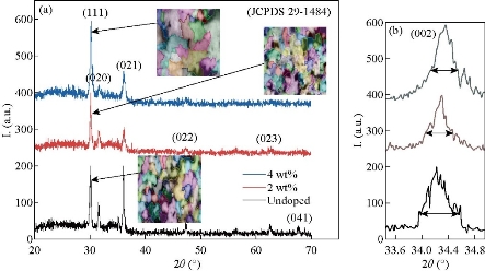
Fig. 1 (a) X-ray diffraction pattern of undoped and V doped SnO2; (b) zoom in the image of the dominant reflection.
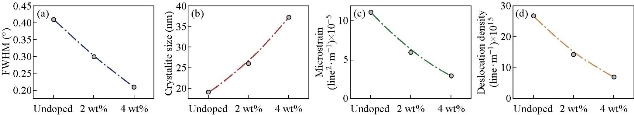
Fig. 2 (a) Full width at half maximum, (b) crystallite size, (c) microstrain, and (d) dislocation density of undoped and V doped SnO2.
Table 1 X-ray diffraction results for undoped and V doped SnO2 films deposited by RF magnetron sputtering at different time duration
|
c (Ǻ) |
b (Ǻ) |
a (Ǻ) |
D (nm) |
FWHM (ᵒ) |
2Ɵ (ᵒ) |
Plane (hkl) |
Samples |
|||
|
Calculated |
Standard |
Calculated |
Standard |
Calculated |
Standard |
|||||
|
5.233 |
5.214 |
5.710 |
5.725 |
4.231 |
4.714 |
19.55 |
0.41 |
30.02 |
(111) |
undoped |
|
5.233 |
5.214 |
5.731 |
5.725 |
4.233 |
4.714 |
26.72 |
0.30 |
30.02 |
(111) |
2 wt% |
|
5.233 |
5.214 |
5.340 |
5.725 |
4.237 |
4.714 |
38.18 |
0.21 |
30.02 |
(111) |
4 wt% |
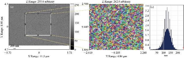
Fig. 3 Scanning electron microscope image of (a) undoped SnO2, (b) magnified and colored image, and (c) distribution of surface heights of a specific area.
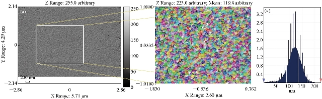
Fig. 4 Scanning electron microscope image of (a) 2wt% doped SnO2, (b) magnified and colored image, and (c) distribution of surface heights of a specific area.
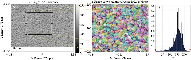
Fig. 5 Scanning electron microscope image of (a) 4wt% doped SnO2, (b) magnified and colored image to determine particle sizes, and (c) distribution of surface heights of a specific area.
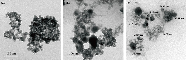
Fig. 6 Transmission electron microscopy image of (a) undoped SnO2, (b) 2% V doped SnO2, and (c) 4% V doped SnO2.
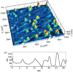
Fig. 7 Atomic force microscopy (AFM) image of undoped SnO2: (a) 3D image 2 × 2 µm, and (b) X-Y scaling for inspection area.
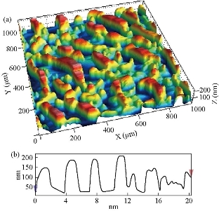
Fig. 8 Atomic force microscopy image of 2 wt% SnO2: (a) 3D image (2×2) µm; (b) XY scaling for inspection area.
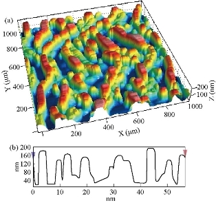
Fig. 9 Atomic force microscopy image of the 4wt% SnO2: (a) 3D image 2 × 2 µm; (b) X-Y scaling for inspection area.
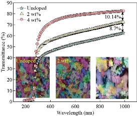
Fig. 10 Transmittance spectrum of the undoped and V doped SnO2 films deposited by spray pyrolysis technique (SPT).
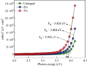
Fig. 11 Optical energy gap of the undoped and V doped SnO2 films deposited by spray pyrolysis technique.
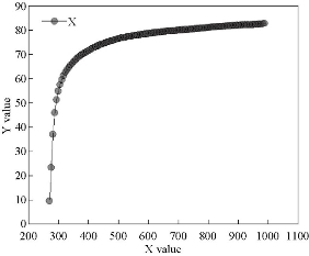
Fig. 12 The mathematical model of the experimental transmittance.
Table 2 a, b, c, d and e values for mathematical models of the transmittance
|
Exponential (a, b, c, d and e) y = a + b/x + c/x2 + d/x3 + e/x4 |
||||||
|
Coefficient of determination (r2) 0.9826434567 |
||||||
|
a |
37.58556758 |
3.514706514 |
10.69379973 |
30.68528602 |
44.48584914 |
0.00000 |
|
b |
84195.32845 |
7247.701779 |
11.61683124 |
69966.20783 |
98424.44907 |
0.00000 |
|
c |
-8.9654e+07 |
5.29754e+06 |
-16.9237190 |
-1.0005e+08 |
-7.9254e+07 |
0.00000 |
|
d |
3.41614e+10 |
1.63239e+09 |
20.92721012 |
3.09566e+10 |
3.73662e+10 |
0.00000 |
|
e |
-4.4786e+12 |
1.79858e+11 |
-24.9009809 |
-4.8317e+12 |
-4.1255e+12 |
0.00000 |
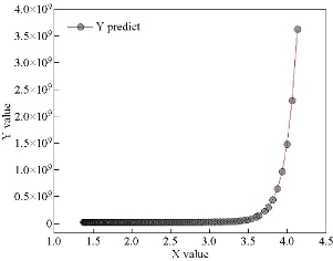
Fig. 13 The mathematical model of the experimental energy gap value.
Table 3 a, b and c value for mathematical models of the energy gap
|
Exponential (a, b and c) y = a + b × Exp(-x/c) |
||||||
|
Coefficient of determination (r2) 0.9954478797 |
||||||
|
a |
2.6258e+07 |
2.71663e+06 |
9.665647820 |
2.08783e+07 |
3.16377e+07 |
0.00000 |
|
b |
0.002248271 |
0.000778029 |
2.889702825 |
0.000707563 |
0.003788979 |
0.00459 |
|
c |
-0.14707494 |
0.001830076 |
-80.3654678 |
-0.15069898 |
-0.14345089 |
0.00000 |
Conclusions
The process of doping tin oxide with vanadium led to improving crystal structure to a degree that all numbers of secondary reflections disappeared and the intensity of the dominant reflection increased with a decrease in the transmittance percentage and the energy gap. The energy gap decreased from 3.82 eV for pure SnO2 thin film to 3.48 eV for 4wt.% vanadium doped SnO2 film.
Acknowledgments
Authors would like to extend their thanks and gratitude to the Department of Physics at the College of Science of the Mustansiriyah University and the Department of Physics at the College of Education of the Mustansiriyah University.
References
Copyright© Shawki Khalaph Muhammad, Ehssan Salah Hassan, Kameran Yasseen Qader, Khalid Haneen Abass, Sami Salman Chiad, and Nadir Fadhil Habubi. This is an open-access article distributed under the terms of the Creative Commons Attribution License, which permits unrestricted use, distribution, and reproduction in any medium, provided the original author and source are credited.

|
Nano Biomedicine and Engineering. Copyright © Shanghai Jiao Tong University Press |
 |