Review
Application of Graphene in Surface-Enhanced Raman Spectroscopy
Jie Chang, Xiao Zhi *, Amin Zhang
Institute of Nano Biomedicine and Engineering, Shanghai Engineering Center for Intelligent Diagnosis and Treatment Instrument, Department of Instrument Science and Engineering, School of Electronic Information and Electrical Engineering, Shanghai Jiao Tong University, 800 Dongchuan Road, Shanghai 200240, P. R. China.
* Corresponding author. E-mail: zhixiao@sjtu.edu.cn
Received: Mar. 21, 2017; Accepted: Mar. 28, 2017; Published: Mar. 28, 2017.
Citation:Jie Chang, Xiao Zhi, and Amin Zhang, Application of Graphene in Surface-Enhanced Raman Spectroscopy. Nano Biomed. Eng., 2017, 9(1): 49-56.
DOI: 10.5101/nbe.v9i1.p49-56.
Abstract
Since the two-dimension structural graphene was discovered in 2004, the researches involved in graphene have and will continue to develop actively because of the excellent properties of graphene. Raman spectroscopy is a quick and precise characterization technique for investigating material properties in material science. Meanwhile, surface-enhanced Raman scattering (SERS) consumingly impacts on surface science owing to its extremely high sensitivity at single molecule level. However, SERS has not been an expected powerful analytical technique due to a variety of technical limitations. Here we briefly review some critical progresses in the development of surface-enhanced Raman scattering (SERS) and various applications of graphene in SERS in recent years.
Keywords: Graphene; Surface-enhanced Raman spectroscopy; Raman scattering
Graphene
Graphene is a monolayer two-dimensional honeycomb crystal with carbon atomic thickness [1]. It can stack to form a three-dimension structural graphite, curl into one-dimensional carbon nanotube, or wrap to zero-dimensional C60 Buckminsterfullerene [2, 3] (Fig. 1). Graphene was firstly obtained by micro-mechanical stripping process; this method can easily get high-quality graphene crystals for further theoretical and experimental researches [4]. As an ideal two-dimensional atomic crystal, graphene possesses many excellent properties such as high electrical conductivity and thermal conductivity, huge surface area, very high Young's modulus and tensile strength. The above advantages make graphene applicable in broad potential fields, including micro-nano electronic devices, optoelectronic detectors, structural and functional composite materials, energy storage and so on [5]. Graphene is a representative semi-metallic semiconductor material [7], and also is almost transparent [8]. To a large extent, the highly internal impurities and scarcely structural defects promote electron mobility rate in graphene by reducing the electron scattering in transport process, 10 times higher than silicon [9]. The resistivity of graphene is lower than that of silver [10]. Graphene has very low Johnson noise (Johnson noise is generated by the thermal vibrations of the carriers inside the electric conductor), so graphene can be used as a channel for the field effect transistor [11]. Excellent electrical properties and low Johnson noise make graphene useful for sensitive sensing devices, for example, for detecting adsorbed molecules from surrounding environment. High conductivity and light transmittance also grant graphene the great potential applications in transparent electrodes, touch screen, liquid crystal display, organic solar cells, organic light-emitting diodes, etc. With a huge surface area, graphene can be used for hydrogen storage. Due to abundant hydrophilic group, graphene oxide can be used as biomolecular carriers for drug and gene delivery in biomedical field [12]. Now, the preparation of graphene commonly used physical and chemical methods: micro-mechanical stripping [9], liquid exfoliation [13, 14], axial cutting carbon nanotube [15], chemical vapor deposition (CVD) [16, 17], crystal epitaxial growth [18] and oxidation-reduction method [19].
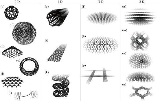
Fig. 1 Molecular models of different types of sp2-like hybridized carbon nanostructures exhibiting different dimensionalities [6].
Surface-Enhanced Raman Scattering (SERS)
Indian physicist Raman in 1928 discovered the light inelastic scattering effect of Raman scattering: monochromatic light irradiation will occur in the molecular surface scattering; a small part of the scattered light energy exchanges with the molecules; the wavelength of the spectrum will change. This spectrum is named “Raman spectroscopy” [20] (Fig. 2). The sharp peaks appear in the spectrum, which characterize the molecular structure of the chemical, and have the functions of qualitative analysis and discrimination of similar substances, which can be used as an effective method for identification of unknown chemicals [21]. Raman spectroscopy is a rapid and non-destructive characterization of material crystal structure, electronic band structure, phonon energy dispersion and electron-phonon [22, 23]. For carbon materials of graphite, graphene, carbon nanotube, C60 and diamond, Raman spectroscopy has been a most popular characterization technique [24, 25]. Raman spectroscopy belongs to molecular vibration spectrum likes as infrared spectroscopy, and can reflect the characteristics of molecular structure. But Raman signal is very weak; the intensity of the incident light intensity is only about 10-10 [26]. In 1974, Fleischmann et al. [27] obtained high-quality Raman spectra of pyridine molecules adsorbed on rough silver electrode surface compared with Raman scattering signals of the same number of pyridine in the solution phase. In 1977, Van Duyne et al. [28] found that the Raman scattering signal of the pyridine on the rough silver surface increased by about one million times. This phenomenon is called surface-enhanced Raman scattering (SERS). Surface-enhanced Raman spectroscopy has been widely used in surface science, chemical analytical and biomolecular detection. As an excellent tool for the characterization of various surfaces (interfaces) (solid-liquid, solid-gas and solid-solid interfaces), SERS can provide information at the molecular level, such as the binding, configuration, orientation of the molecule (ions) on the surface and the surface structure of the material. It is generally believed that there are two surface-enhanced Raman scattering mechanisms of electromagnetic enhancement and chemical enhancement [20]. Under the two simultaneous enhancement mechanisms, Raman enhancement factor is even up to 109~1014. Electromagnetic enhancement is based on the localized plasma oscillations produced by excitation of the metal substrate in the external field. When the external field frequency and the plasma resonance frequency coincide, the metal surface of the field strength is enhanced. The region of effective enhancement is localized near the particle surface, because the effect of field enhancement is attenuated by r-3. Theoretically, the intensity of Raman enhancement is the fourth power of the electromagnetic field and the fourth power of the polarizability [29]. The study of chemical enhancement mechanism is still relatively limited, lacking very strong evidence of the ability of chemical enhancement. According to general opinions, due to the strong interaction between molecules and substrate, the resonant charge transfer occurs and enhances the Raman signal of the molecules [30]. Surface-enhanced Raman spectroscopy has some characteristics compared with conventional Raman spectroscopy: Firstly, the signal intensity is limited by the surface-enhanced Raman spectroscopy substrate of noble metals (gold, silver and copper) and alkali (lithium, sodium and potassium). Secondly, the vibration modes of different molecules are different. The intensity of most Raman vibrational peaks of the molecules does not change significantly, but the relative intensity of the enhanced peaks is different. Finally, it is necessary to select the optimum excitation wavelength according to different substrate materials [31].
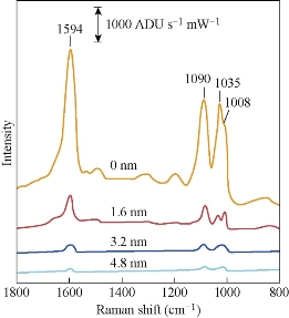
Fig. 2 Surface-enhanced Raman spectra of pyridine adsorbed to silver film over nanosphere samples treated with various thicknesses of alumina (0.0 , 1.6, 3.2 and 4.8 nm) [20].
Applications of Graphene in SERS
Raman spectra of graphene
The main Raman peaks of Graphene are D peak, G peak and 2D peak. The D peak involves the scattering process of incident photons in graphene, reflecting the degree of disorder of graphene. The more defects, the higher the degree of disorder and the stronger D peak. The position of G peak, relating to the Fermi level position of graphene, can be used as an important criterion for reduction degree of graphene and doping type and degree. If carrier concentration becomes high, the G peak blue-shifts and half-width narrows. 2D peak represents the degree of graphitization, with the increase of doping concentration and defects, intensity of the 2D peak weakened [5, 32]. Based on these Raman spectral fingerprints, Raman spectroscopy can be used to identify the number of graphene layers, detect the types of defects and doping level [32]. For different layers of graphene, the 2D peak displays varied shape, position and intensity, and there is a linear relationship between the intensity and the number of layers of graphene [33] (Fig. 3). Koh et al. [34] demonstrated how graphene layers can be identified based on the G peaks of graphene. Cançado et al. [35] found that with the edge of the different graphene, the Raman spectrum of the D characteristic band is different. This D-band is due to a defect and a phonon caused by the second-order Raman scattering. The D-band is therefore determined by the structure of the edges regardless of whether the edge of the graphene is zigzag or armchair. Krauss et al. [36] have succeeded in obtaining graphene with predominantly zigzagged edges by anisotropy of the edges, which also demonstrates that the zigzag edge does not contribute to the D-band. There are also reports that the D-bands of the two edges of graphene have no significant difference. In addition to the graphene edges, defects in artificial graphene also lead to the appearance of D and 2D Raman bands. The graphene doping degree also has important influence on the properties of graphene [37]. Different methods and environmental conditions can get graphene with different doping degrees [5]. Different points of the same graphene also have varying degrees of doping. Raman spectroscopy is important for detecting graphene doping, and can help us understand electron-phonon interaction of graphene. Although the chemical dopant effect of natural graphene is important in most cases, we will only discuss electrical-induced doping samples here. Yan et al. [38] found that G band and 2D band shift of graphene greatly depended on the charge density induced by the electric field effect. In short, Raman spectroscopy is a sensitive tool for detecting graphene layers, edges, disordered numbers and dopants. The difference in the behavior of electrons and phonons in graphene provides an interesting platform for the study of Raman scattering effects. However, the graphene synthesis and functionalization technologies are still in development, which provides a good opportunity to Raman characteristics.
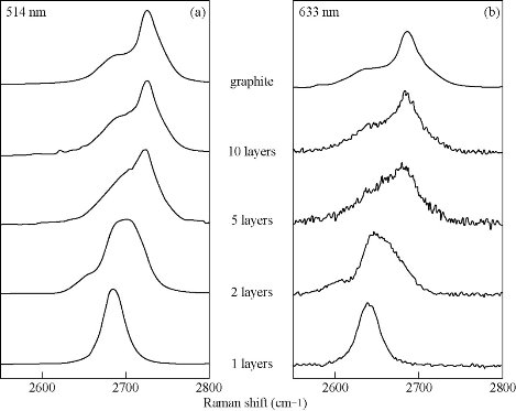
Fig. 3 Evolution of the Raman spectra at 514 nm (a) and 633 nm (b) with the number of layers [33].
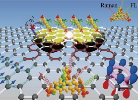
Fig. 4 Graphene as a platform for SERS [32]
Role of graphene in SERS
In addition to pyridine, a wide variety of SERS probes have been explored. The probe parameters are fixed when probes own Raman behavior. Qualitative and quantitative information about the composition of a sample is taken into account. As we investigate the basic details of SERS effect, the most important consideration is the careful selection of probes [32] (Fig. 4).
Explore the fine structure of graphene
Most of properties of graphene are closely related to the structure, and it has been found that the fine structure of graphene can reveal the Raman spectrum well. The Raman intensity of graphene was easily affected by substrate. Generally, a silicon with an oxide layer of 300 nm was selected as a SERS substrate. The oxide layer is essential for the optical visibility of the graphene and Raman enhancement intensity based on a thin-sheet interference effect [39-42]. The thickness of the oxide layer is correlated with the interference enhancement [43]. Chen et al. [44] obtained a plasma resonance surface enhancement of 1000 times in a Si/Ag/Al2O3/graphene structure. Domke et al. [45] obtained a 1 million-fold localized electromagnetic enhancement in SPM tip region. Lee et al. [46] found that the D band changes of graphene on an Au layer due to surface Raman enhancement. Wang et al. [47] found that the tip is not only a introducer of defect, but also a signal amplifier of Raman enhancement.
The relationship between matrix structure and SERS
It is important to develope reliable quantitative surface-enhanced Raman methods and develop deep understanding of plasma Raman resonance in chemical physics. However, there are few studies in this field, because of the difficulty in the arrangement and stability of molecular probes under the conditions of surface-enhanced Raman spectroscopy. Graphene provides a new substrate for related investigations: two-dimensional graphene is homogeneous and chemically inert. Schedin et al. [48] fabricated different gold nanoparticle arrays to demonstrate the structural independence of surface-enhanced Raman spectroscopy. Xu et al. [49] investigated the relationship between surface-enhanced Raman spectra of graphene and the thickness of vacuum-evaporated gold film. Niue et al. [50] added a layer of alumina between the gold nanoparticles and the SiC epitaxial graphene. They found that the enhancement factor was exponentially related to the distance between the graphene and the gold nanoparticles.
Graphene as a SERS substrate
The acquisition of Raman signals of molecules from their fluorescence background has been a problem for a long time. Nonresonant excitation can save the problem to some extent; nevertheless, this method can cause sensitivity losses. The spectra of molecules adsorbed on graphene are able to change in comparison with their intrinsic spectra. Xie et al. [51] firstly observed the fluorescence quenching of the fluorescent dye adsorbed on graphene, but still obtained the Raman spectra of the same molecules. Thus, the graphene substrate provides an effective way to measure the Raman spectra of fluorescent dyes under resonant excitation, which is generally difficult to achieve. Cui et al. [52] developed a SERS sensor comprising of gold nanoparticles and reduced graphene oxide to detect fourteen volatile organic compounds (VOCs) biomarkers in the breath to distinguish early gastric cancer and advanced gastric cancer (Fig. 5). Liu et al. [53] discovered the graphene-enhanced Raman spectroscopy (GERS) effect by comparing the Raman signals of popular Raman probes (phthalocyanine, rhodamine 6G, protoporphyin IX and crystal violet) on monolayer graphene and on a SiO2/Si substrate using vacuum evaporation or solution soaking. The intensities of Raman signals on monolayer graphene are much stronger than that on a SiO2/Si substrate. They attributed this enhancement to the charge transfer between the graphene and the molecules, which results in a chemical enhancement (Fig. 6). The influence phenomenon in graphene-enhanced Raman spectroscopy has also been studied. Zhang et al. [54] found that the variation of Raman intensity of graphene on different thicknesses of SiO2/Si substrates followed the interference law. The variation of the Raman intensity of the Raman probes molecules on graphene and on SiO2/Si substrate also well followed the interference law. However, for the GERS system, the Raman intensity of the molecules is obviously enhanced compared to the molecules on SiO2/Si substrates. Begliarbekov et al. [55] studied the fluorescence spectra of R6G on graphene antidot superlattices. The fluorescence from deposited dye molecules was found to strongly quench as a function of increasing antidot filling fraction, whereas it was enhanced in unpatterned but electrically backgated samples. This contrasting behavior is strongly indicative of a built-in lateral electric field that accounts for fluorescence quenching as well as p-type doping.
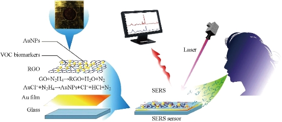
Fig. 5 Schematic diagrams of SERS sensor for detecting volatile organic compounds (VOCs) in the breath for early gastric cancer diagnosis [52].
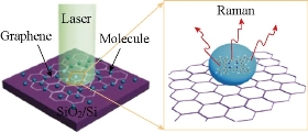
Fig. 6 Schematic illustration of the molecules on graphene and a SiO2/Si substrate, and the Raman experiments [53].
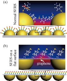
Fig. 7 (a) Molecules on a normal SERS substrate; and (b) molecules on flat SERS substrate mediated by a graphene sheet [49].
Graphene composites as SERS substrates
With the increase of the sensitivity of SERS, the internal interference has become an important problem. Gold and silver as popular SERS substrates usually are a natural catalysts for various chemical reactions. They easily introduce negative effects into SERS by substrate-to-molecular charge transfer, photo-induced damage and metal catalytic reaction. Owing to the chemical inertness of graphene, graphene can be used to prevent contact between metal substrates and molecules as a thin, pin-hole-free coating layer in SERS [49]. However, graphene does not cause significant attenuation of electromagnetic enhancement of SERS (Fig. 7).
Conclusions
Graphene has a great enhancement effect for surface-enhanced Raman spectroscopy. However, the application of graphene in SERS is not random. Surface-enhanced Raman spectroscopy experiments also need to be designed well. So far, graphene has become an important material for SERS by virtue of its unique structure, physical and chemical properties. In-depth studies on graphene involved SERS are expected to offer deeper understandings of the SERS effect, as well as a better balance on sensitivity, reproducibility and selectivity in the performance of SERS. Yet, the main challenge are the following aspects: controllable functionalization of graphene with expectant functions, the design and integration of Raman probes, plasmonic metal structures, more reliable qualitative/quantitative evaluation of SERS, and more convenient/compatible SERS techniques. It is optimistic that graphene continues to play an important role in SERS in the future.
Acknowledgments
This work was supported by National Natural Scientific Fund (No. 81225010), the National Key Basic Research Program (973 Project) (No. 2010CB933901 and 2015CB931802), 863 Project of China (No. 2014AA020700), and Shanghai Science and Technology Fund (No. 13NM1401500).
References
Copyright© 2017 Jie Chang, Xiao Zhi, and Amin Zhang. This is an open-access article distributed under the terms of the Creative Commons Attribution License, which permits unrestricted use, distribution, and reproduction in any medium, provided the original author and source are credited.

|
Nano Biomedicine and Engineering. Copyright © Shanghai Jiao Tong University Press |
 |