Influence of Copper and Zinc Doping on Optical Properties of Nano Nickel Oxide Films Deposited by Sol-Gel Method
Ameera J. Kadhm, Israa Akram Abbas*
Department of Physics, College of Education for Pure Science, Al-Mustansiriyah University, Baghdad, Iraq
*Corresponding author. E-mail: israaaabbas512@gmail.com
Received: Aug. 17, 2022; Revised: Nov. 01, 2022; Accepted: Dec. 01, 2022; Published: Dec. 31, 2022
Citation: A.J. Kadhm, I.A. Abbas. Influence of copper and zinc doping on optical properties of nano nickel oxide films deposited by sol-gel method. Nano Biomedicine and Engineering, 2022, 14(4): 360–366.
DOI: 10.5101/nbe.v14i4.p360-366
Abstract
In this study, nano films of pure NiO and films doped with zinc and copper concertation (1%, 3%, 5%) and their mixture for 5% under 100nm thickness were generated on glass bases using the sol-gel process at a temperature of 298K. The Cu, Zn-doped NiO and nano NiO optical characteristics were examined throughout a wavelength range of 300 to 800 nm, with high transmittance values of 94% in the Vis-NIR. Transmittance films after doped copper and zinc have dropped to 5% (91% and 92%), respectively. The index of refraction, coefficient of extinction, optical conductivity and the dielctric constants (real and imaginary) were also studied. The results show that the optical conductivity of NiO⁚Zn and NiO⁚Cu films increased at the room temperature with increasing the dopant concentrations.
Keywords: Thin films; Doping; Sol-Gel Method; Zn-doping; Cu-doping
Introduction
An excellent example of a p-type semiconductor with a wide band gap energy range of 3.6 to 4.0 eV is nickel oxide (NiO) [1]. NiO is an interesting contender in this class for applications requiring clear conducting p-type oxide semiconductors [1]. The NiO is a fascinating substance that is utilized in solar cells [2], transparent electronics [3], electrochromic devices [3, 4], and as a useful sensor layer for chemical sensors [5]. The following characteristics make NiO particularly appealing: ①excellent durability and electrochemical stability, ② low material cost, ③ promising ion storage material in terms of cyclic stability, ④ a high spin optical density, and ⑤ the ability to be manufactured using a variety of techniques [6–12]. Thin films can be created using a variety of techniques, including the sol-gel method, sputtering, spray pyrolysis [13], and laser deposition. The sol-gel approach is popular because of its benefits, including affordability, simplicity in deposition, simplicity in managing the composition of the films, and simplicity in controlling doping percentage [14–16]. A few papers have concentrated on the synthesis and deposition of zinc-doped NiO thin layers. Additionally, doping with Zn ion can modify the band structure of NiO to affect its optoelectronic performance [17–19].
In this work, we have synthesized the effect of different copper and zinc concentrations on the physical properties of pure and copper and zinc doped NiO thin films deposited by sol-gel technique.
Materials and Preparation
A solution of hexahydrate nickel chloride was prepared with a molar mass of 237.69 g/mol and a concentration of 0.4 mol/L. Take 9.5 g of nickel chloride salt and dissolve it in 100 mL of ethanol, then stir slowly for six hours at room temperature using a German-made magnetic stirrer to ensure that there is no precipitate and complete dissolution of the legal substance in ethanol. The resultant mixed solution was dropped on glass slides using a spin coater apparatus setting to 3000 r/min for 30 s. To remove organic contaminations, the as-deposited NiO films were dried at 100℃ for around 5 mi. The previous procedure was done four times. The same process was used to create Cu and Zn doped NiO films from solutions prepared by adding cooper and zinc to the mixed solution at varying mass fraction of 1%, 3%, and 5%. Finally, all deposited films were annealed in the air for 2 h at 350℃.
Results and Discussion
Optical properties are of great importance in understanding the properties of semiconductors nanostructures, through which it is possible to understand and develop the structure of beams and optical energy gap and know their suitability for practical application. The optical properties of the NiO nanofilm and the films doped with zinc and copper were studied individually and their mixture with mass fraction of 1%, 3%, 5%, deposited on glass bases at a temperature of 298K with a thickness of nanoparticles 100nm, through the spectral change of absorption and transmittance in the range of ultraviolet wavelengths and the region visible and near infrared.
Transmittance
Figure 1 shows the transmittance spectrum of the NiO nano-film and the zinc-doped films with mass fraction of 1%, 3%, 5% within the wavelength range of 300–800 nm. The transmittance shows in two separate zones׃ the first at short wavelengths less than 360nm, where the transmittance increases practically abruptly with increasing wavelength, and the second at longer wavelengths greater than 360nm. In the second region, which is greater than 360nm, we notice that the membrane's permeability is high (up to 94%) throughout the visible region and extends into the near infrared region (that is, in the range of low energies Vis-NIR). This finding qualifies it for using as permeable layers in solar cells, which outperforms the results of a number of researchers who analyzed the NiO compound in the form of a film of nano and non-nano thickness generated using a method similar to the one used in our work, as well as other approaches [20, 21]. After doping the nano-membrane with zinc with mass fraction of 1%, 3%, 5%, the transmittance values started decreasing to reach (91%) for 5% doping at wavelengths greater than 360 nm, i.e., in the low energies Vis-NIR range. As for the copper-doped NiO nano films with the same mass fraction shown in Fig. 2, the transmittance values decreased to 92% upon doping with 5% in the low-energy range Vis-NIR, and this also qualifies them to work as anti-reflection coatings such as permeable layers in solar cells. This behavior is similar to previous research with a clear superiority in the results of the transmittance values for our current study [22, 23]. The decrease in transmittance values with higher doping ratios could be due to the creation of localized quantities of zinc or copper impurities within the energy gap, resulting in an increase in absorbance.
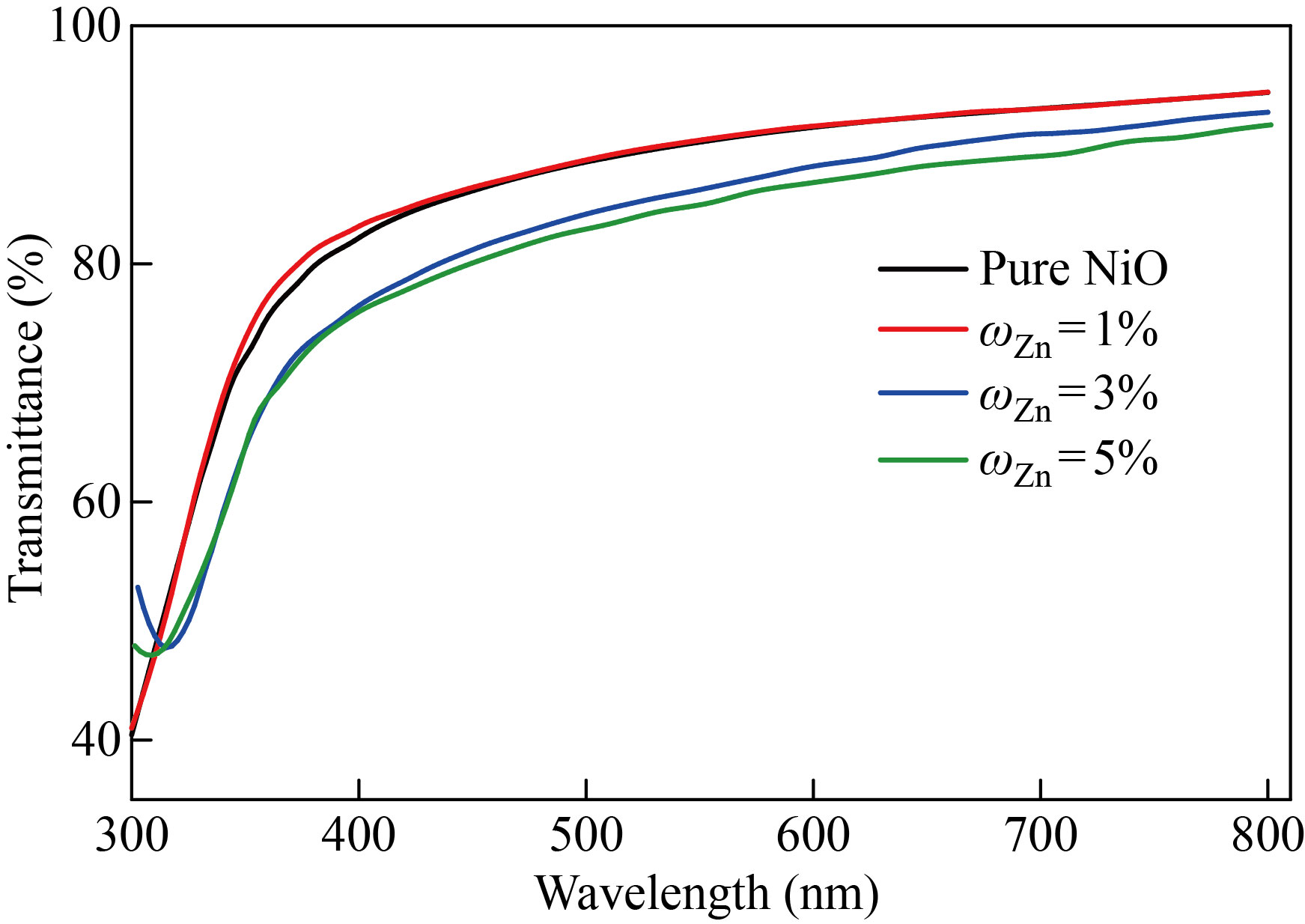
Fig. 1 Transmittance spectrum as a function of the wavelength of pure NiO and NiO׃Zn films with different doping ratios
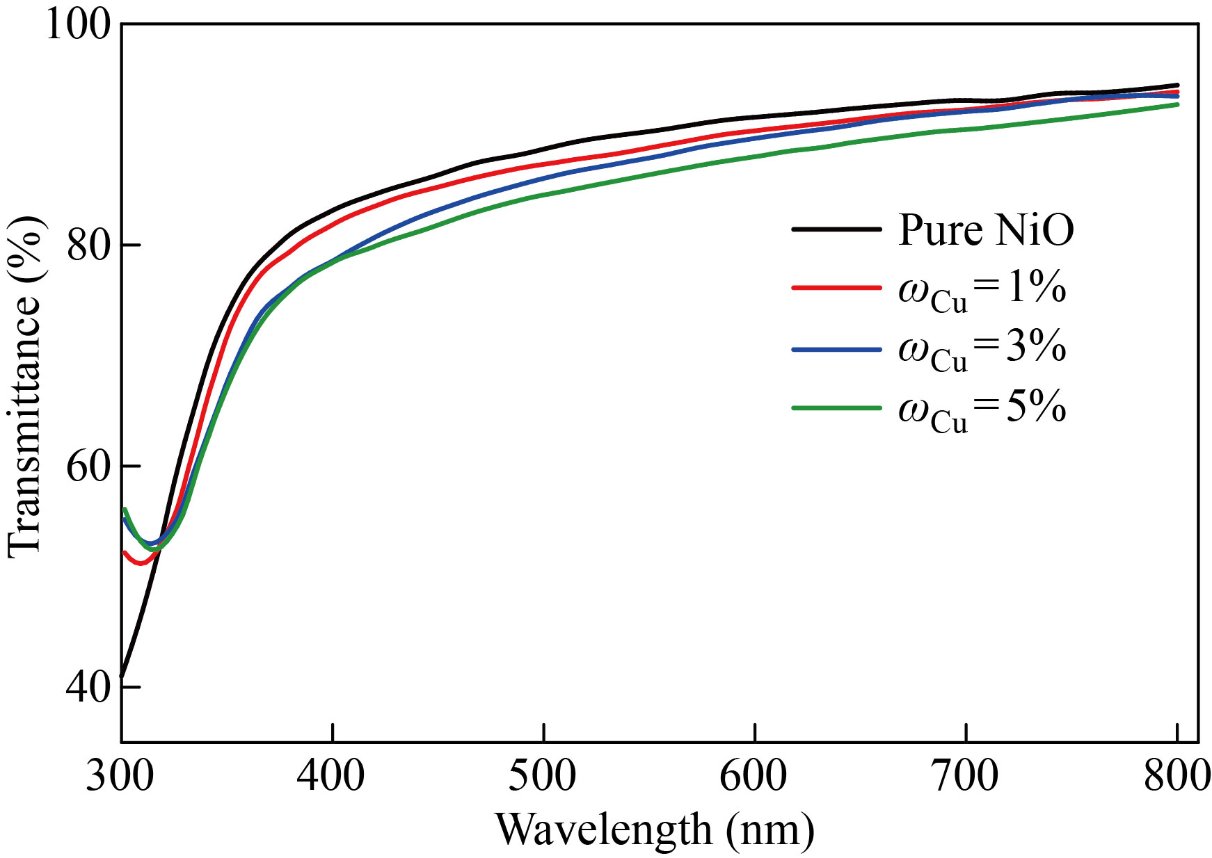
Fig. 2 Transmittance spectrum as a function of the wavelength of pure NiO and NiO׃Cu films with different doping ratios
Absorbance
The strongly permitted optical stimulation of electrons across the energy gap results in a significant increase in absorbance at a wavelength matching the energy gap. The optical absorption edge is the name given to this characteristic of the absorption spectrum. Figures 3 and 4 show the absorption spectra of pure NiO and the NiO׃ Zn films with ratios of 1%, 3%, 5% within the wavelengths of 300–800nm, respectively. The absorbance of all films has a large amount at wavelengths adjacent to the basic absorption edge (320–360nm); then as the wavelength increases the absorbance decreases. The absorbance of the films generally takes low values in the visible and near infrared region. At high wavelengths, the photons of the incident light do not have enough energy to interact with the atoms of the material, and the photon is carried out. In the region of wavelengths less than 320 nm, it crawls towards higher wavelengths (red shift). With the increase in the percentage of distortion, it is assumed that a decrease in the optical power gap is in agreement with previous research [24]. After the wavelength of 320nm, there are no absorption peaks, and this is due to the superior transmittance of the films in that region of the visible spectrum. The absorbance values increase with the increase in the percentages of distortion to increase the grain size and also due to the decrease in the optical energy gap as a result of the energy gap's local concentrations of copper or zinc impurities.
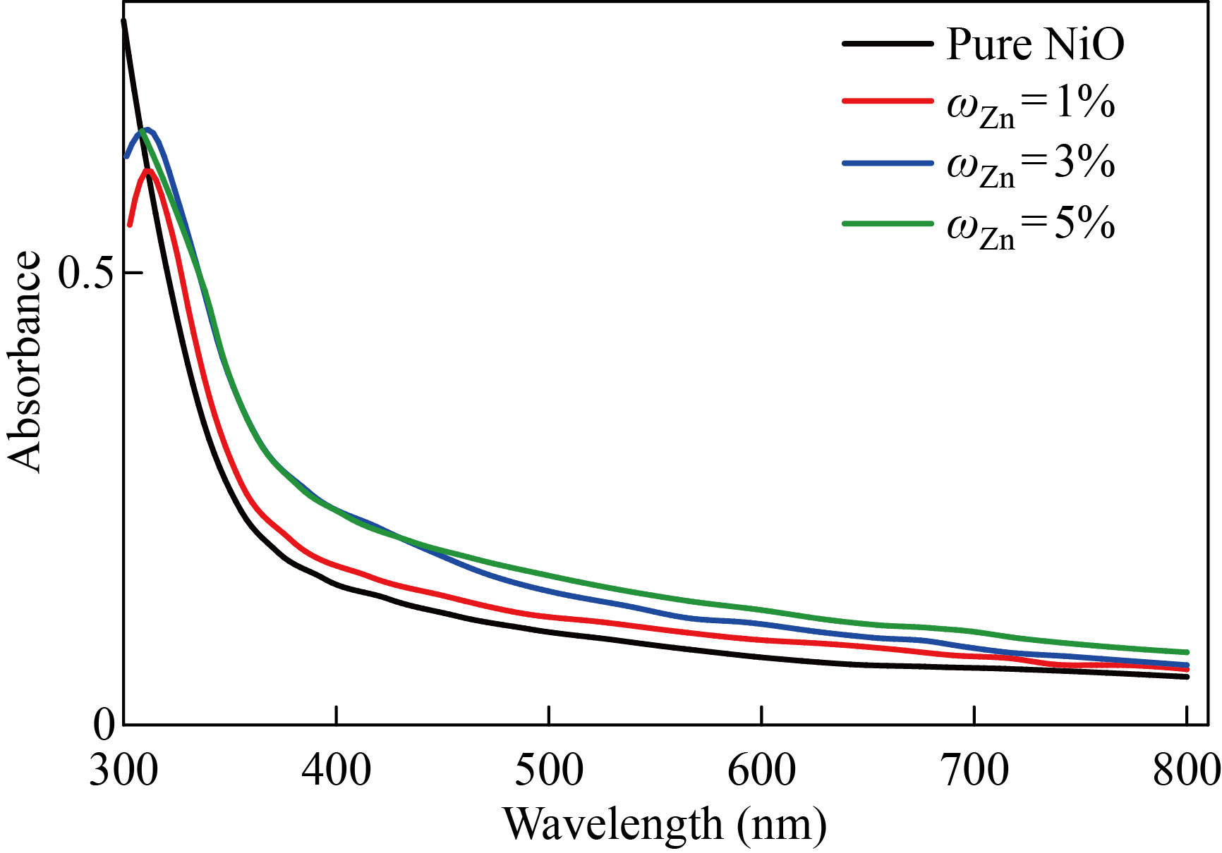
Fig. 3 Absorbance spectrum as a function of the wavelength of pure and NiO׃Zn films with different doping ratios
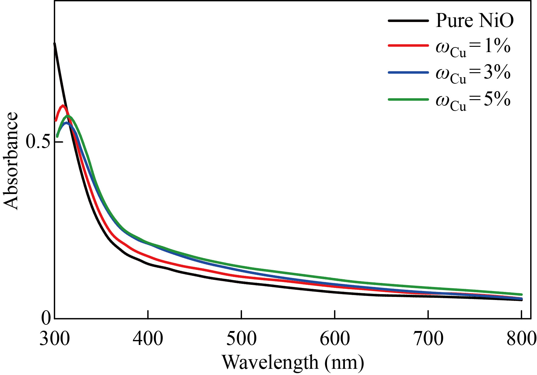
Fig. 4 Absorbance spectrum as a function of the wavelength of pure and NiO׃Cu films with different doping ratios
Optical absorption coefficient
Figures 5 and 6 show the absorption coefficient (α) of the NiO nanofilm and the copper, zinc-doped films versus the incident photon energy (hν). The increase in the absorption coefficient is slowly gradual increase at lower energies. Therefore, these films can be used as anti-reflection coatings in solar cells and reagents at low energies and then increase faster in the higher energies range (3.5–3.8 eV) and (3.5–3.9 eV) respectively. From this increase, it is possible to identify the basic absorption edge and the occurrence of transitions between the valence band and conduction. From Figs. 5 and 6, the coefficient of absorption is about 3×104 cm-1 at the energy gap of 3.5 eV, and this suggests that direct electronic transitions have occurred, which shows a reduction in optical energy gap values, and this is caused by the creation of local levels near the conduction band.
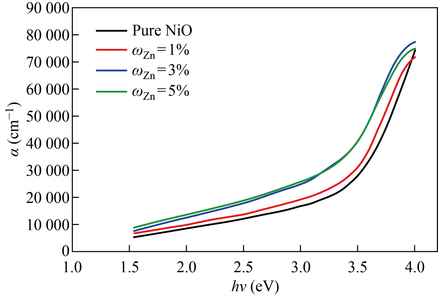
Fig.5 The absorption coefficient as a function of the photon energy of pure and NiO׃Zn films with different doping ratios
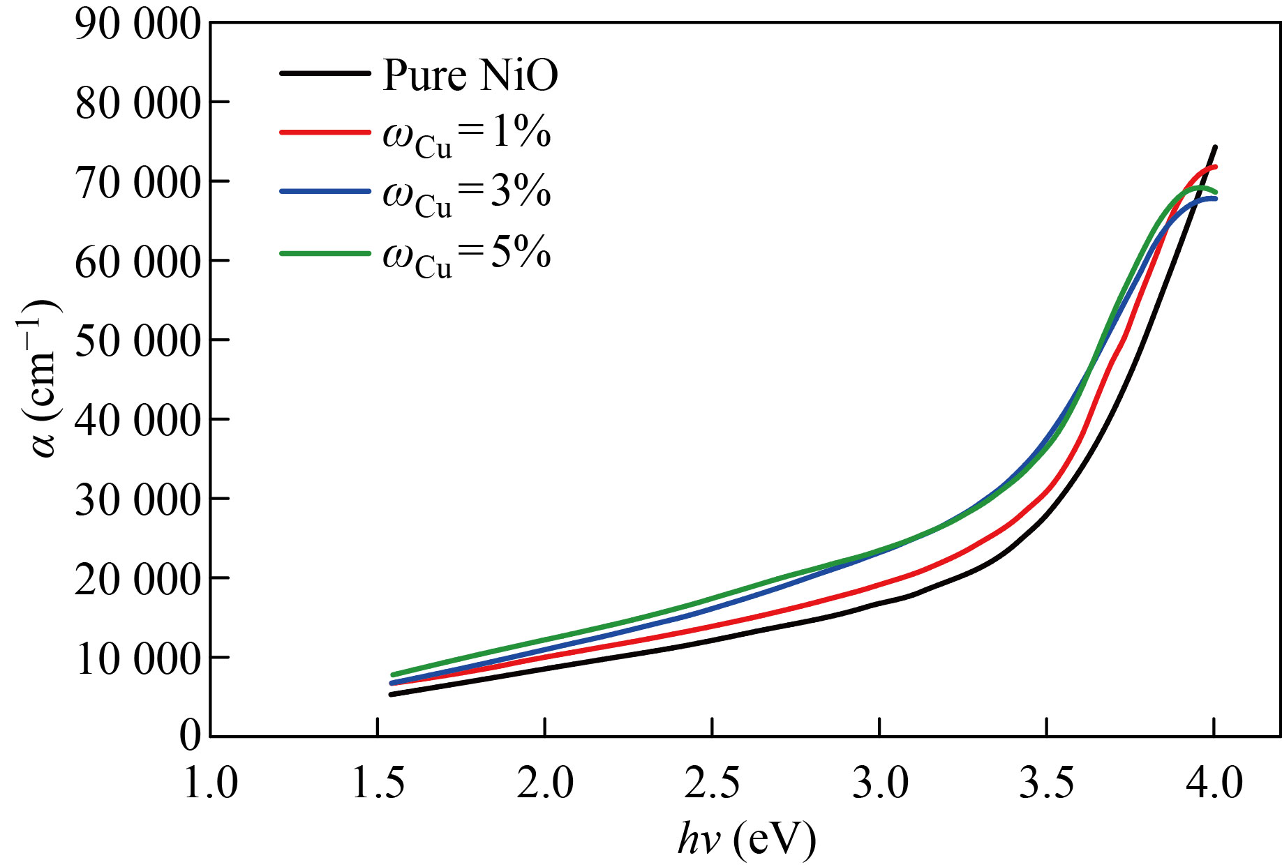
Fig.6 The absorption coefficient as a function of the photon energy of pure and NiO׃Cu films with different doping ratios
Optical energy gap
The allowed direct energy gap was calculated by extending the straight (tangent) part of the curve until it intersected the photon energy axis hv at hνα=0. The permitted direct optical energy gap values for the NiO nanofilm were 100nm and 3.73 eV, as shown in Fig. 7, which are within the range of conventional energy gap values for NiO films (3.6–4 eV). The permitted direct optical energy gap values for pure NiO were 100nm and 3.73eV, as shown in Fig. 7, which are within the range of conventional energy gap values for NiO films (3.6–4 eV). The rise in charge carriers, or the increase in Zn and Cu concentration in the deposited films, causes changes in the homogeneity and density of the local levels, which causes a drop in the optical energy gap values. In addition, the decrease in the optical energy gap values may be related to the percentage increase in the grain size, on the basis of which the optical energy gap values appear for the case of doping with zinc less than in the case of copper.
Table 1 The optical energy gap for pure NiO, NiO׃Zn and NiO׃Cu
Mass fraction | Optical gap (eV) Zn | Optical gap (eV) Cu |
Pure NiO | 3.37 | 3.37 |
1 % | 3.58 | 3.61 |
3 % | 3.42 | 3.49 |
3 % | 3.41 | 3.42 |
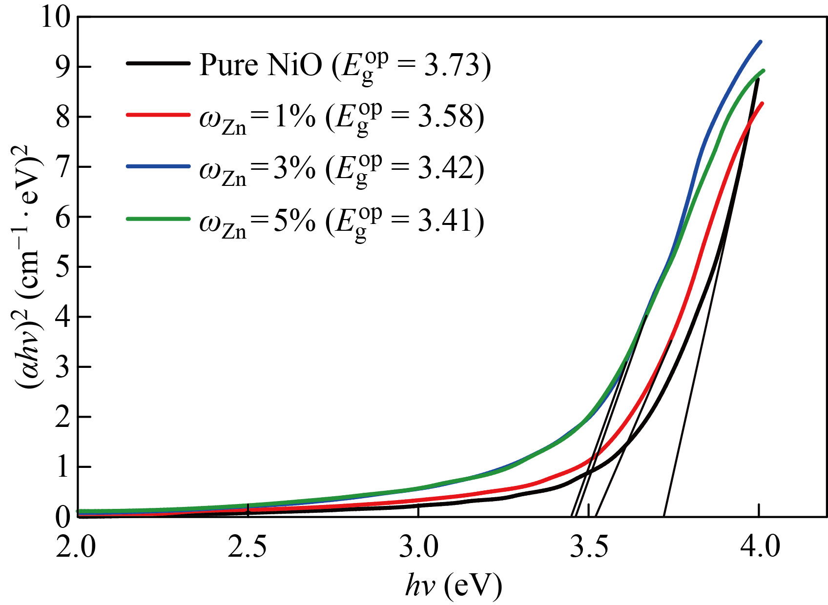
Fig. 7 The optical energy gap of the pure and NiO׃Zn films with different doping ratios
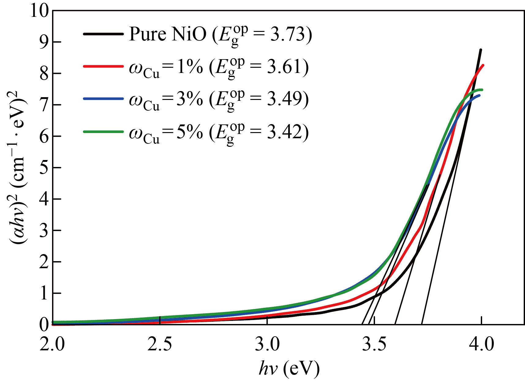
Fig. 8 The optical energy gap of the pure NiO and NiO׃Cu films with different doping ratios
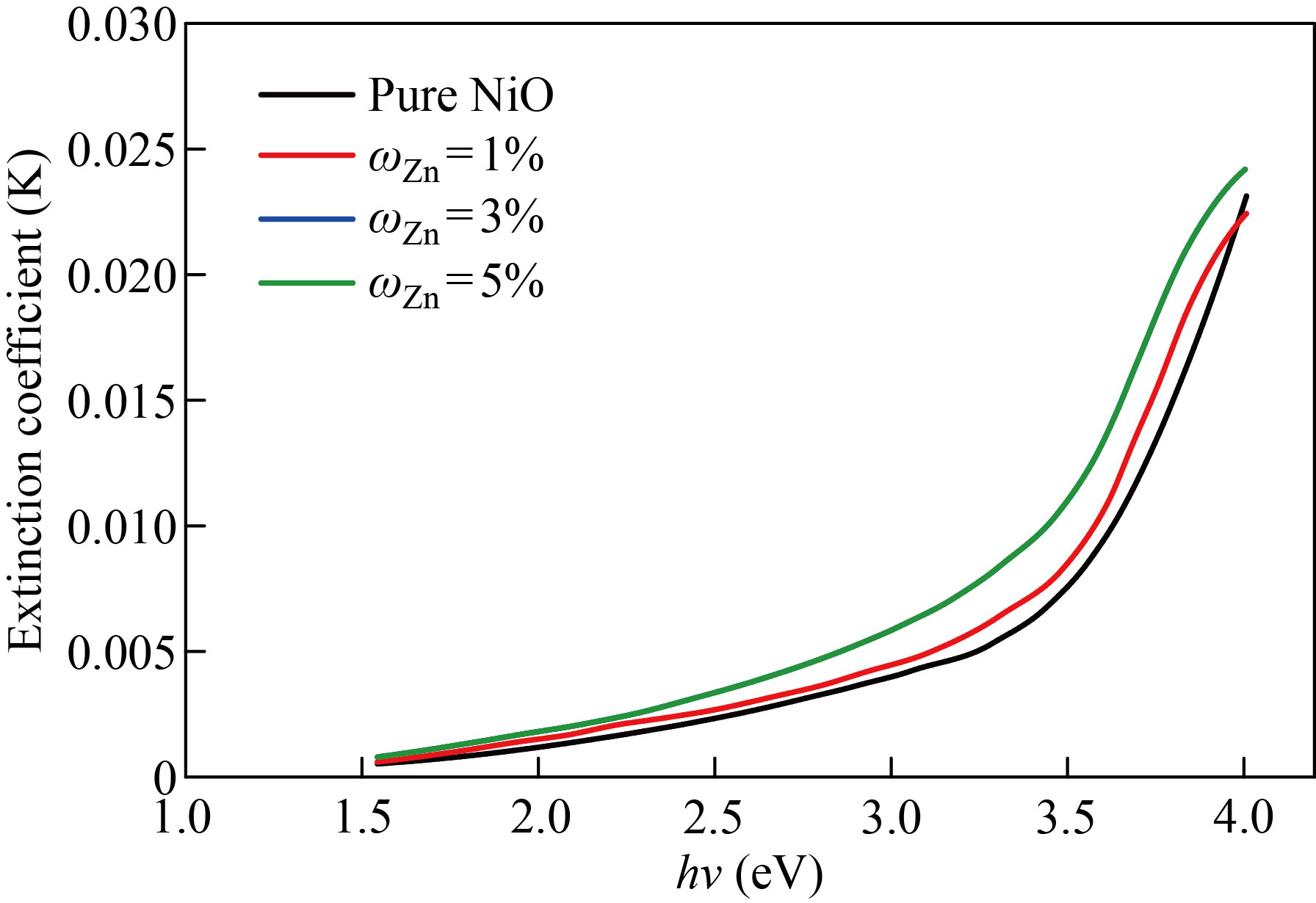
Fig. 9 The extinction coefficient pure NiO and NiO׃Zn films with various doping ratios as a function of incident photon energy
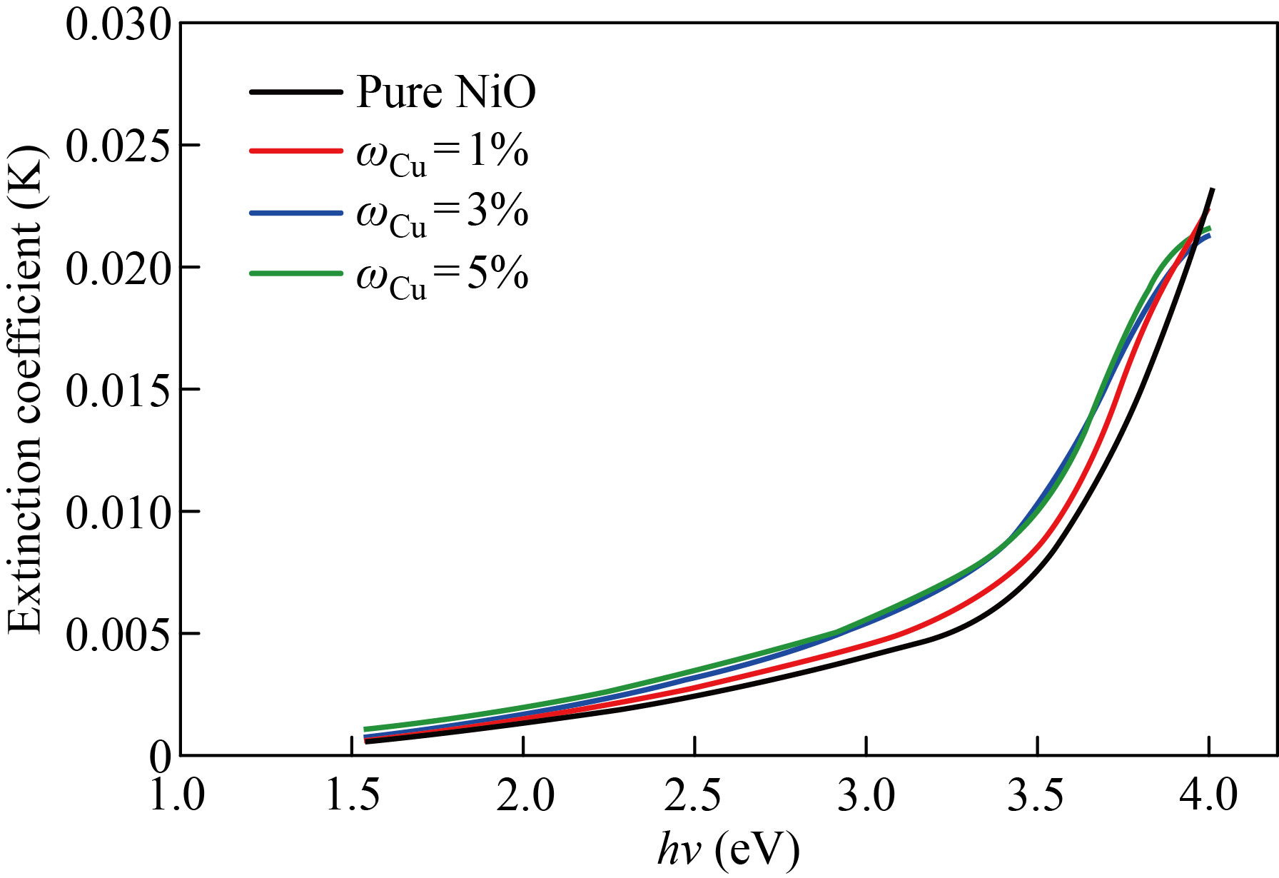
Fig. 10 The extinction coefficient pure NiO and NiO׃Cu films with various doping ratios as a function of incident photon energy
Refractive and extinction coefficients
The extinction coefficient of pure NiO, NiO׃Zn and NiO׃Cu films doped with zinc and copper in mass fraction of 1%, 3%, 5% as a function of incident photon energy (h) are depicted in Figs. 9 and 10, respectively. We notice that the values of the damping coefficient increase with the increase in the energy of the photon, and this increase in the values of the damping coefficient is a result of the increase in the values of the absorption coefficient. Figures 11 and 12 show the relationship between the refractive index and the photon energy of the NiO nanofilm and the zinc-copper doped films with mass fraction of 1%,3%,5%, respectively. We notice an increase in the refractive index with an increase in the energy of the incident photon and for the different percentages of addition, and this is explained in the light of the inverse relationship between the refractive index and wavelength and this behavior agreement with previous research [24].
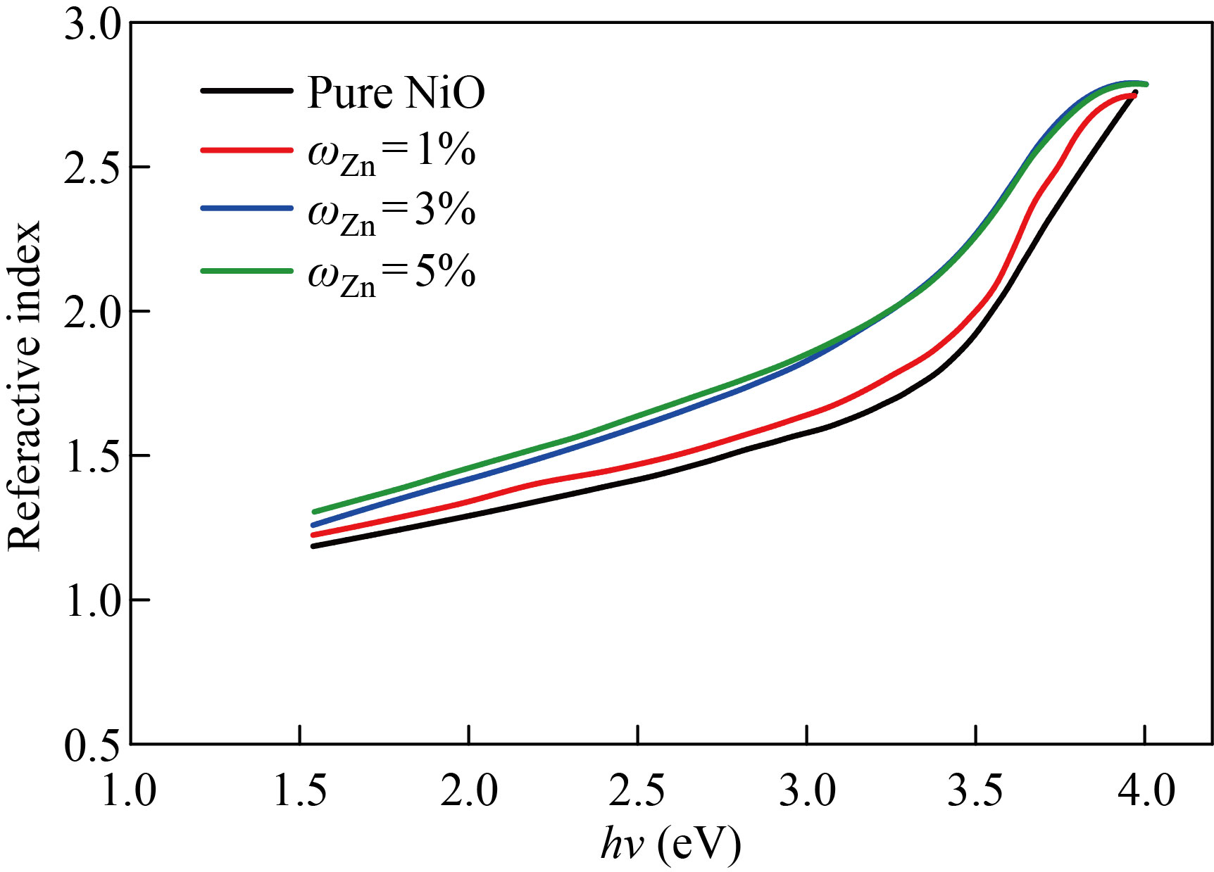
Fig. 11 The index of refraction as a function of input photon energy for NiO nanomembranes and Zn-doped films with varied doping ratios
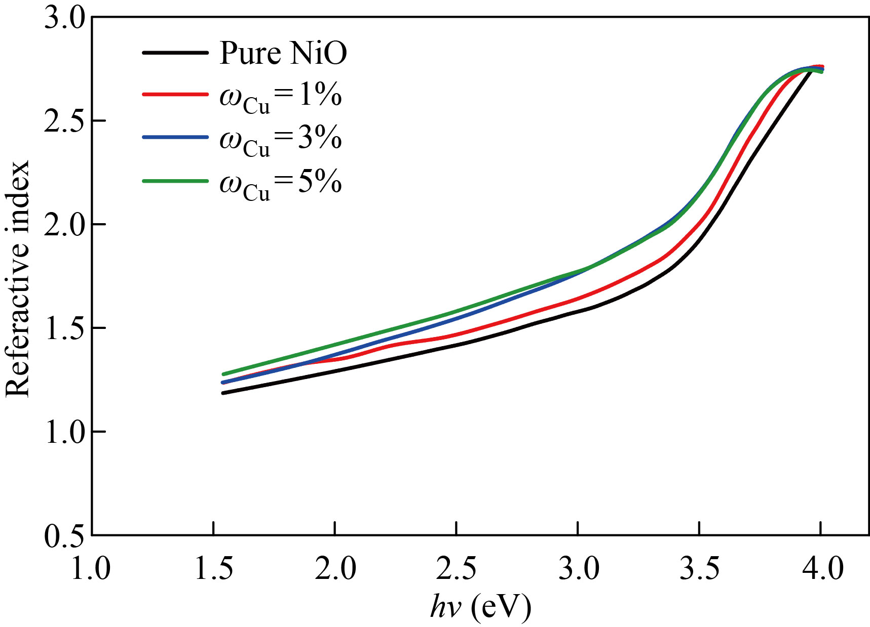
Fig. 12 The index of refraction as a function of input photon energy for NiO nanomembranes and Cu-doped films with varied doping ratios
Complex dielectric constant
The NiO nanoparticles and zinc-copper doped films with mass fraction of 1%, 3%, 5% are shown in Figs. 13 and 14 to demonstrate how the real part of the dielectric constant changes as a function of wavelength. The behavior of the real dielectric constant curve resembles that of the refractive index curve to some extent. The curve starts decreasing at high wavelengths, but after doping, the real dielectric constant values decrease with the increase in doping ratios. The effect of the damping index is slightly compared to the effect of the index of refraction. Figures 15 and 16 display the variation in the imaginary part of the dielectric constant as a function of wavelength for zinc-copper doped films and NiO nanofilms, respectively. As we note that the curve behaves similar to the curve of the damping coefficient, but after doping, we notice that the value of the imaginary dielectric constant increases with the increase in the percentage of doping.
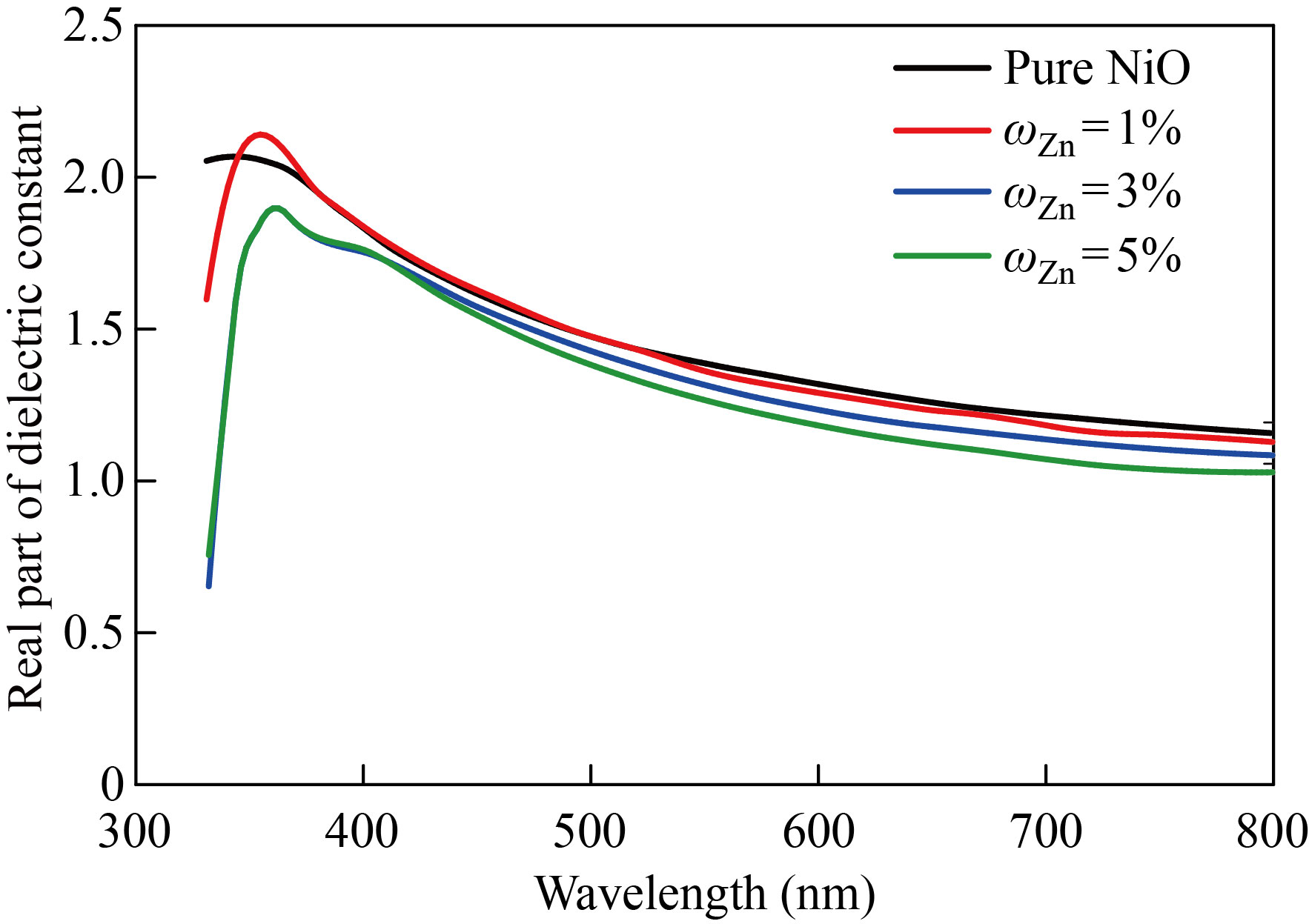
Fig. 13 The NiO nanomembrane and Zn-doped films with various doping ratios’ values of the real dielectric constant as a function of wavelength
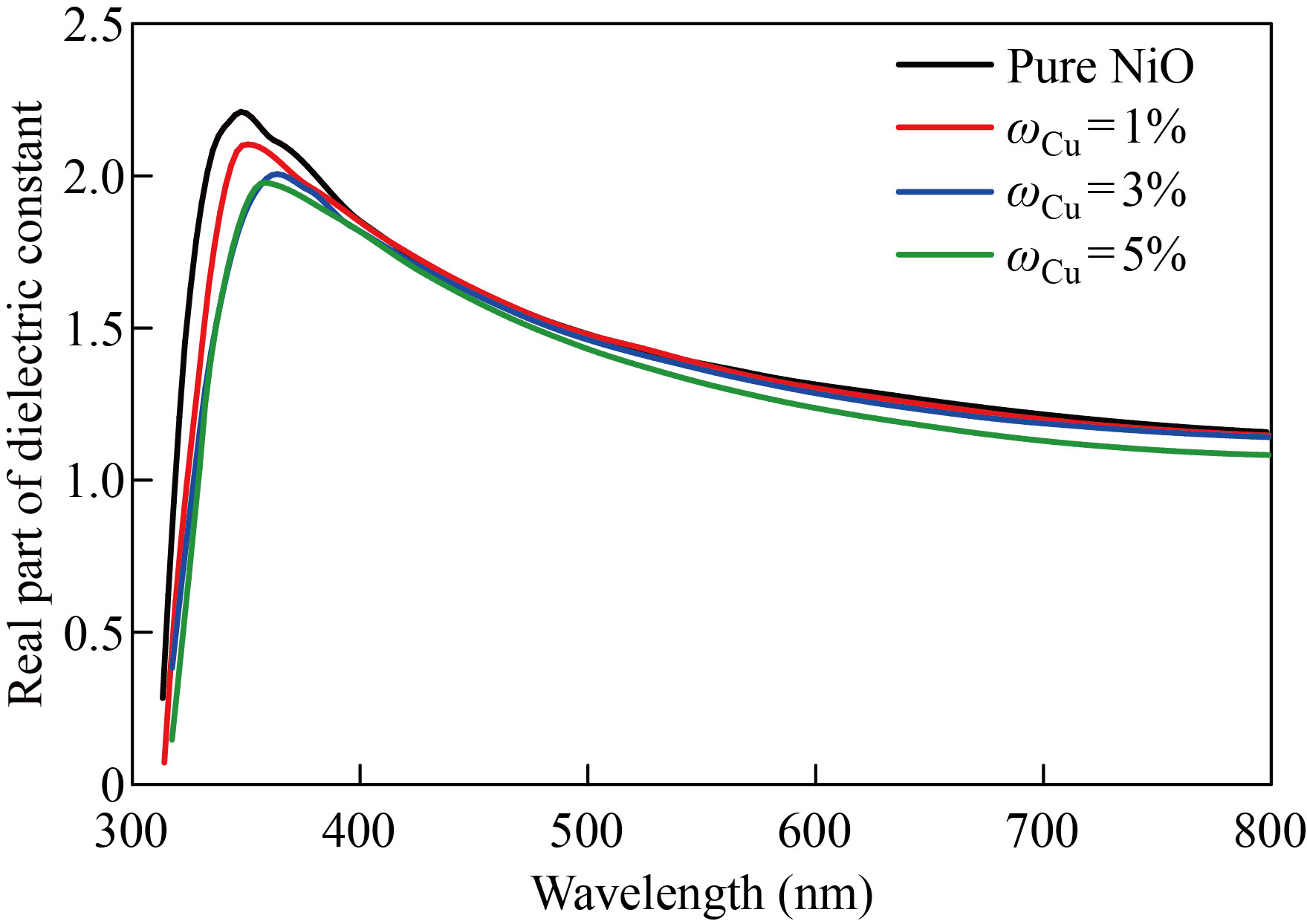
Fig. 14 The NiO nanomembrane and Cu-doped films with various doping ratios’ values of the real dielectric constant as a function of wavelength
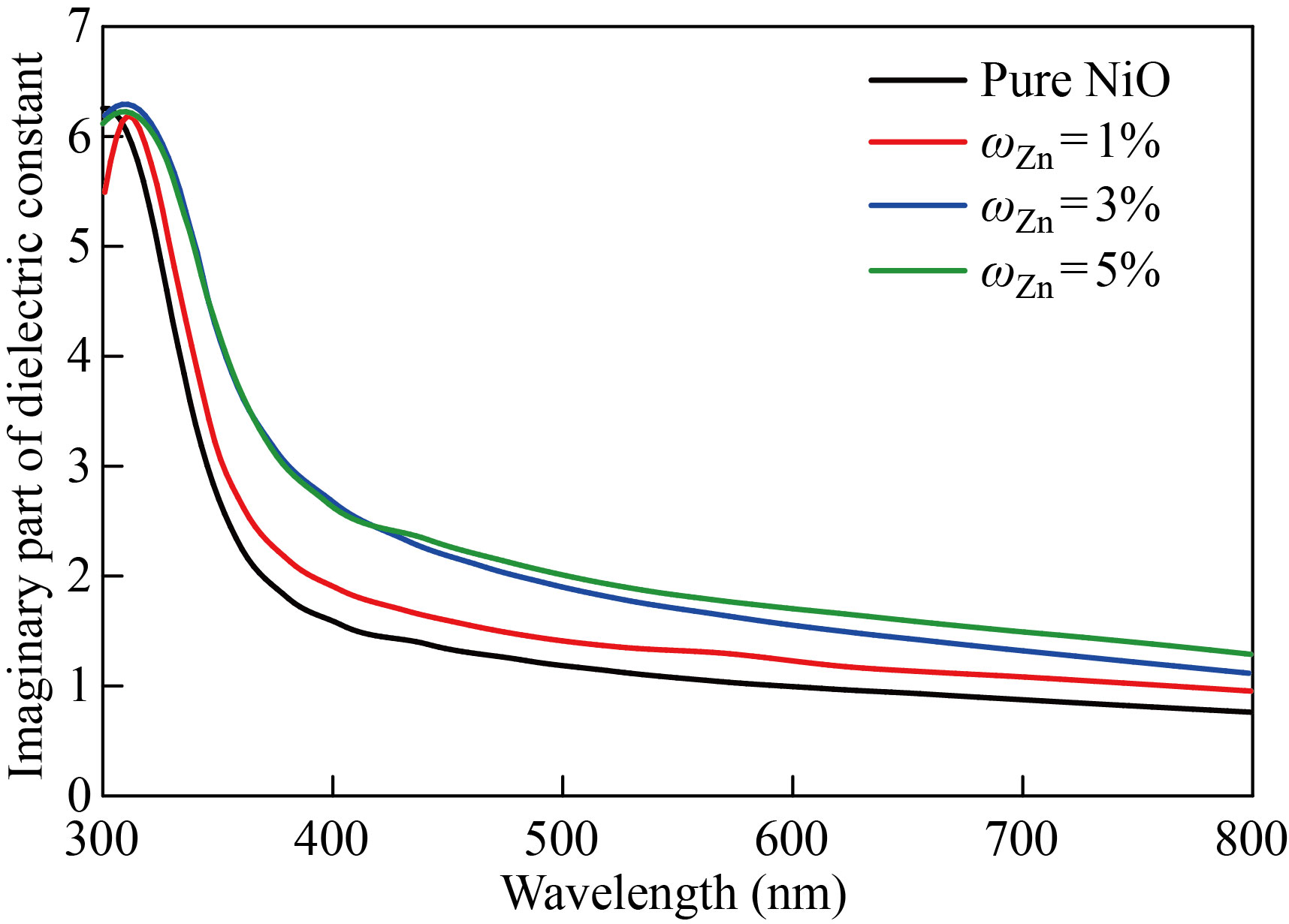
Fig. 15 The imaginary dielectric constant values of the NiO nanomembrane and Zn-doped films with varying doping ratios as a function of wavelength
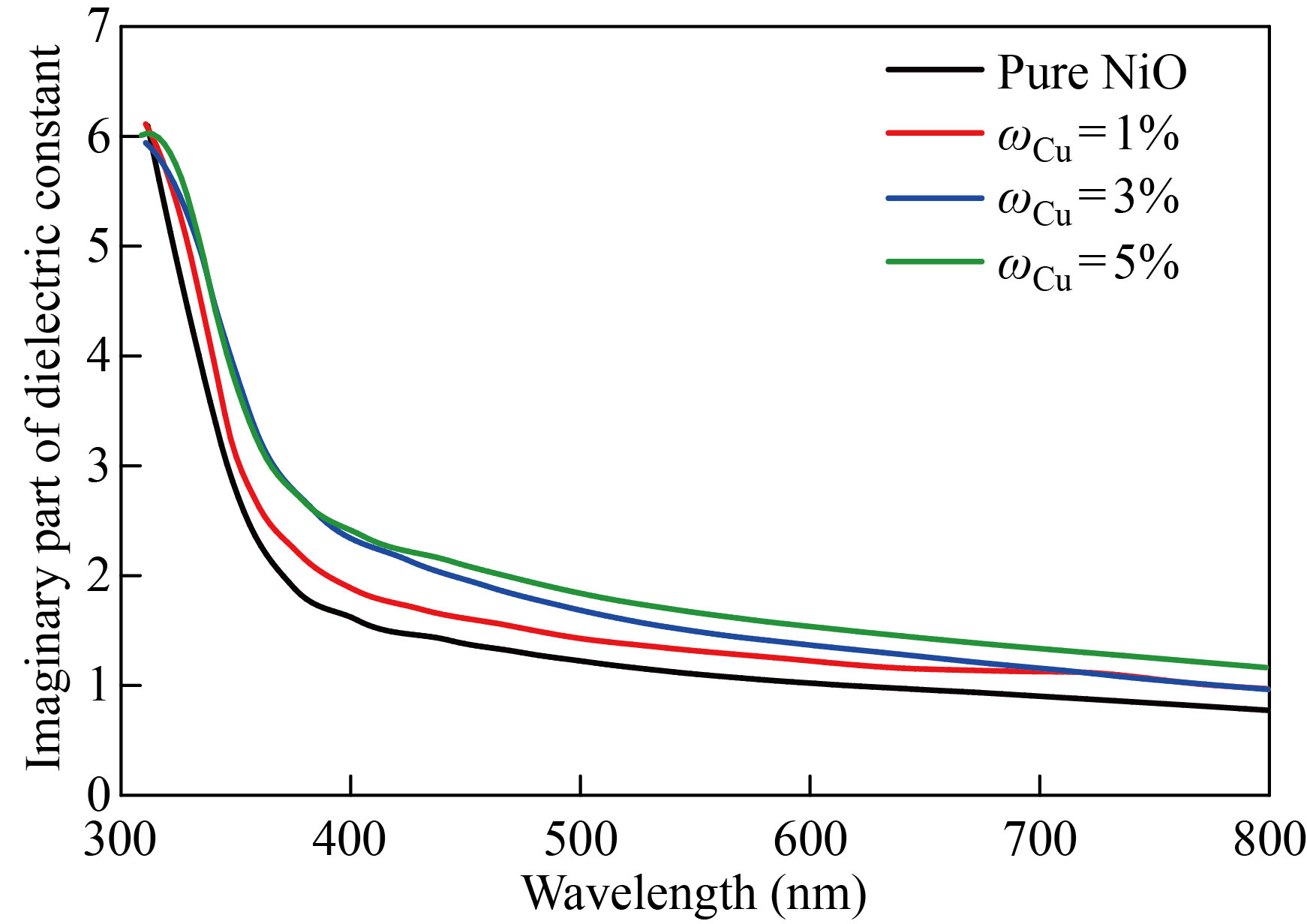
Fig. 16 The imaginary dielectric constant values of the NiO nanomembrane and Cu-doped films with varying doping ratios as a function of wavelength
Optical conductivity
Figures 17 and 18 change the optical conductivity of the NiO nanofilm and the Zn-Cu-doped films in mass fraction of 1%, 3%, 5% as a function of the incident photon (hν). From the figure, it increases dramatically at higher power energies. As for the effect of doping, it shows an increase in the conductivity in an orderly manner, and this indicates a significant increase in the conductivity of the membrane and this behavior agreement with previous research [24].
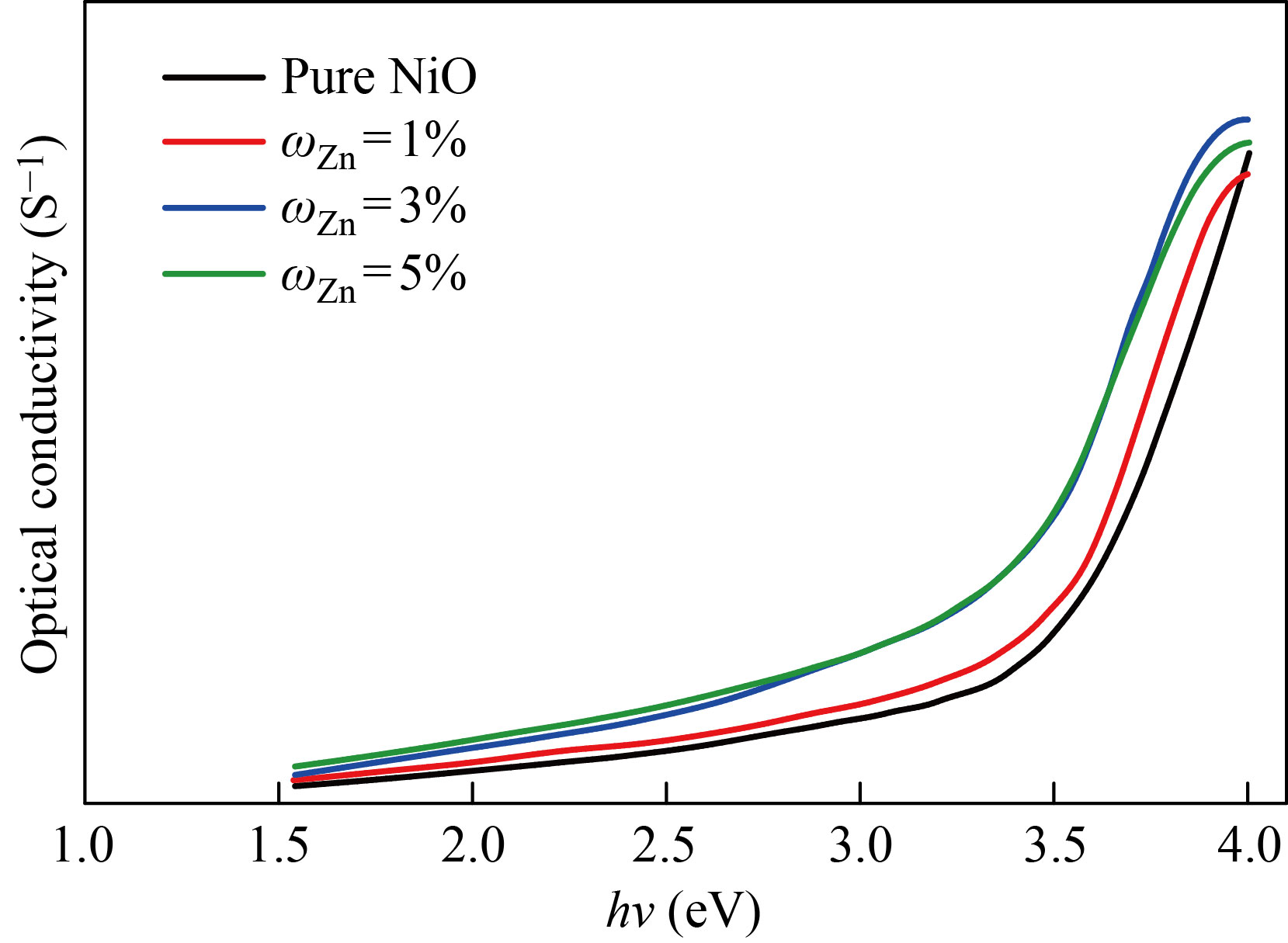
Fig. 17 Optical conductivity values of NiO nanomembranes and Zn-doped films with varied doping ratios as a function of incident photon energy
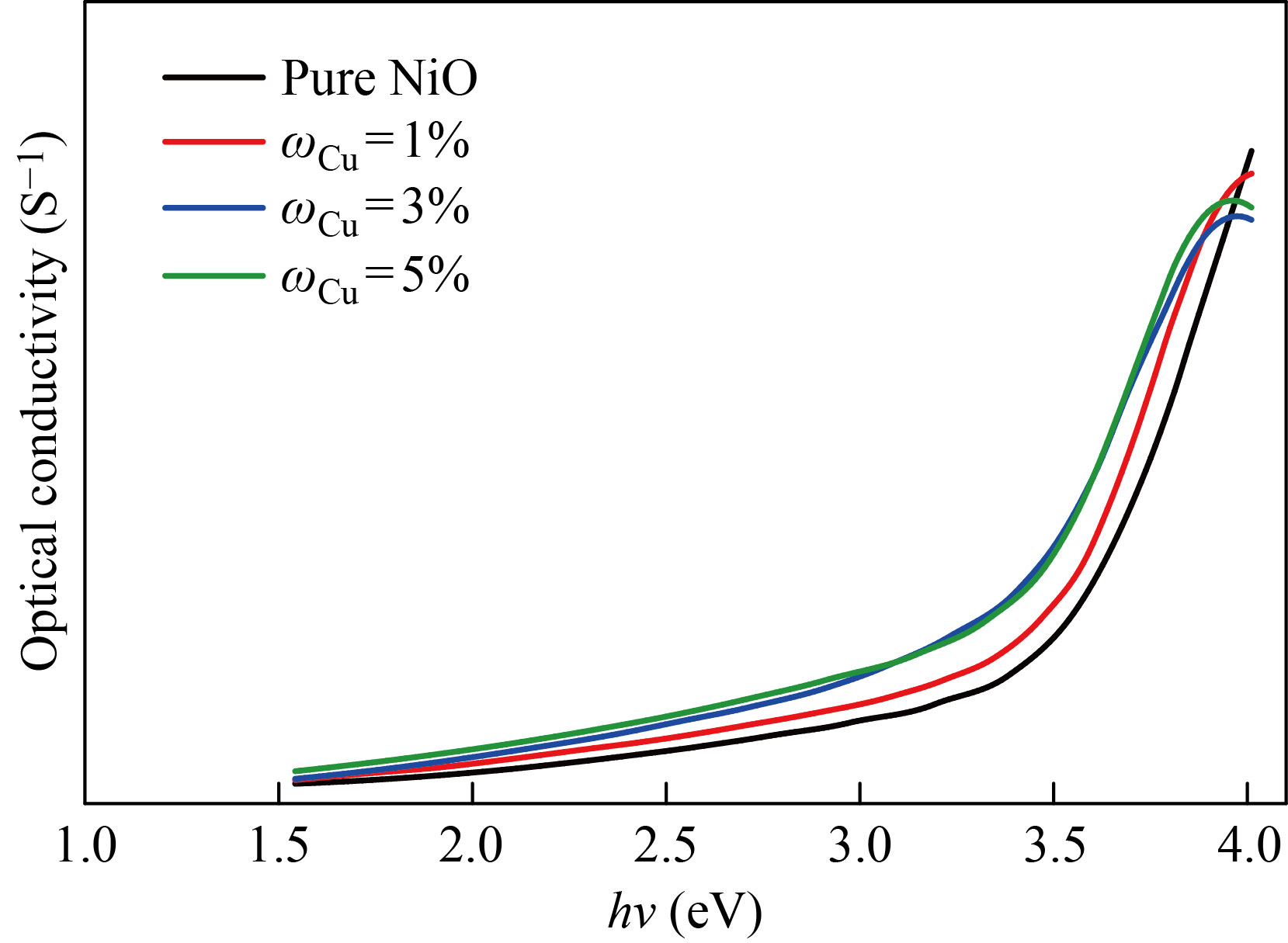
Fig. 18 Optical conductivity values of NiO nanomembranes and Cu-doped films with varied doping ratios as a function of incident photon energy
Conclusion
In this study, nano films of pure (NiO) and films doped with zinc and copper mass fraction of 0, 1%, 3%, 5% and their mixture for 5% under 100 nm thickness were prepared on glass bases using sol-gel method. The optical properties of nanocomposites have been studied: the transmittance, absorbance, absorption coefficient, refractive and extinction coefficients, dielectric constant (real, imaginary) and the optical conductivity. By calculating the transmittance of the NiO nanoparticle, it was found that it has the highest value of transmittance (94%) within the low energies range (Vis-NIR), while the permeability of the films after doping with zinc and copper decreased to reach at 5% to 91% and 92%, respectively, and this qualifies them to be suitable to work as anti-reflection coatings to improve the efficiency of the solar cell and that the dielectric constant in its real and imaginary parts increases with increasing wavelength.
References
[1] D. Adler, J. Feinleib. Electrical and optical properties of narrow-band materials. Physical Review B, 1970, 2: 3112–3134. https://doi.org/10.1103/physrevb.2.3112
[2] N. Kikuchi, K. Tonooka. Electrical and structural properties of Ni-doped Cu2O films prepared by pulsed laser deposition. Thin Solid Films, 2005, 486: 33–37. http://dx.doi.org/10.1016/j.tsf.2004.12.044
[3] A.N. Banerjee, K.K. Chattopadhyay. Recent developments in the emerging field of crystalline p-type transparent conducting oxide thin films. Progress in Crystal Growth and Characterization of Materials, 2005, 50: 52–105. https://doi.org/10.1016/j.pcrysgrow.2005.10.001
[4] M. Kitao, K. Izawa, K. Urabe, et al. Preparation and electrochromic properties of RF-sputtered NiOx films prepared in Ar/O2/H2 atmosphere. Japanese Journal of Applied Physics, 1994, 33: 6656. https://doi.org/10.1143/jjap.33.6656
[5] K. Yoshimura, T. Miki, S. Tanemura. Nickel oxide electrochromic thin films prepared by reactive DC magnetron sputtering. Japanese Journal of Applied Physics, 1995, 34: 2440. https://doi.org/10.1143/jjap.34.2440
[6] H. Kumagai, M. Matsumoto, K. Toyoda, et al. Preparation and characteristics of nickel oxide thin film by controlled growth with sequential surface chemical reactions. Journal of Materials Science Letters, 1996, 15: 1081–1083. https://doi.org/10.1007/BF00274914
[7] K.D. Lee, W. Jung. Effect of substrate temperature on the electrochromic properties and cyclic durability of nickel oxide films. Journal of the Korean Physical Society, 2004, 45: 447–454.
[8] E. Avendaño, L. Berggren, G.A. Niklasson, et al. Electrochromic materials and devices: Brief survey and new data on optical absorption in tungsten oxide and nickel oxide films. Thin Solid Films, 2006, 496: 30–36. https://doi.org/10.1016/j.tsf.2005.08.183
[9] P.S. Patil, L.D. Kadam. Preparation and characterization of spray pyrolyzed nickel oxide (NiO) thin films. Applied Surface Science, 2002, 199: 211–221. https://doi.org/10.1016/s0169-4332(02)00839-5
[10] C.M. Lampert. Large-area smart glass and integrated photovoltaics. Solar Energy Materials and Solar Cells, 2003, 76: 489–499. https://doi.org/10.1016/S0927-0248(02)00259-3
[11] J. Nagai. Advances in research and applications of electrochromic smart windows. Solid State Ionics, 1990, 40-41: 383–387. https://doi.org/10.1016/0167-2738(90)90363-V
[12] K.D. Lee. Influence of film thickness on the chemical stability of electrochromic tungsten oxide film. Journal of the Korean Physical Society, 2001, 38(1): 33.
[13] G, Kenanakis, . Influence of precursor type, deposition time and doping concentration on the morphological, electrical and optical properties of ZnO and ZnO: Al thin films grown by ultrasonic spray pyrolysis. Thin Solid Films, 2014, 555: 62–67. http://dx.doi.org/10.1016/j.tsf.2013.10.015
[14] B.W. Shivaraj, H.N.N. Murthy, M. Krishna, et al. Effect of annealing temperature on structural and optical properties of dip and spin coated ZnO thin films. Procedia Materials Science, 2015, 10: 292–300. https://doi.org/10.1016/j.mspro.2015.06.053
[15] M. Caglar, F. Yakuphanoglu. Structural and optical properties of copper doped ZnO films derived by Sol–gel. Applied Surface Science, 2012, 258: 3039–3044. https://doi.org/10.1016/j.apsusc.2011.11.033
[16] J.G. Lv, K. Huang, X.M. Chen, et al. Optical constants of Na-doped ZnO thin films by Sol–gel method. Optics Communications, 2011, 284: 2905–2908. https://doi.org/10.1016/j.optcom.2011.01.075
[17] M.D. Irwin, D.B. Buchholz, A.W. Hains, et al. p-Type semiconducting nickel oxide as an efficiency-enhancing anode interfacial layer in polymer bulk-heterojunction solar cells. Proceedings of the National Academy of Sciences, 2008, 105: 2783–2787. https://doi.org/10.1073/pnas.0711990105
[18] R.S. Kate, S.C. Bulakhe, R.J. Deokate. Co doping effect on structural and optical properties of nickel oxide (NiO) thin films via spray pyrolysis. Optical and Quantum Electronics, 2019, 51: 319. http://dx.doi.org/10.1007/s11082-019-2026-2
[19] S. Parwani, P. Dubey, R.C. Dixit, et al. AIP Conference Proceedings, 2019, 2100: 020092.
[20] N.F.A. Shammary. Optical characteristics of NiO thin film on glass formed by chemical spray pyrolysis. Journal of Kufa-Physics, 2010, 2(1): 22–27.
[21] A.J. Hassan. Journal of Modern Physics, 2014, 5: 2184–2191.
[22] A.K. Srivastava, S. Thota, J. Kumar. Preparation, microstructure and optical absorption behaviour of NiO thin films. Journal of Nanoscience and Nanotechnology, 2008, 8: 4111–4115. https://doi.org/10.1166/jnn.2008.an36
[23] A.A. Al-Ghamdi, W.E. Mahmoud, S.J. Yaghmour, et al. Structure and optical properties of nanocrystalline NiO thin film synthesized by Sol–gel spin-coating method. Journal of Alloys and Compounds, 2009, 486: 9–13. https://doi.org/10.1016/j.jallcom.2009.06.139
[24] L. Zhao, G. Su, W. Liu, et al. Optical and electrochemical properties of Cu-doped NiO films prepared by electrochemical deposition. Applied Surface Science, 2011, 257: 3974–3979. http://dx.doi.org/10.1016/j.apsusc.2010.11.160
Copyright© Ameera J. Kadhm and Israa Akram Abbas. This is an open-access article distributed under the terms of the Creative Commons Attribution License (CC BY), which permits unrestricted use, distribution, and reproduction in any medium, provided the original author and source are credited.